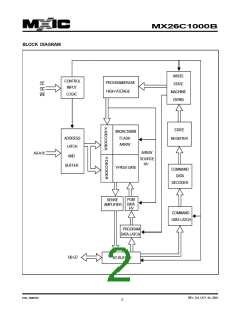
MX26C1000B
EPROMTM is built on an innovative cell concept in which
over erasing the memory cell is impossible.
force 12.0 ±0.5 V on address line A9 of the device.
Two identifier bytes may then be sequenced from the
device outputs by toggling address line A0 from VIL to
VIH. All other address lines must be held at VIL during
auto identify mode.
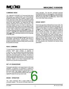
DATA WRITE PROTECTION
Byte 0 ( A0 = VIL) represents the manufacturer code,
and byte 1 (A0 = VIH), the device identifier code. For
the MX26C1000B, these two identifier bytes are given
intheModeSelectTable. Allidentifiersformanufacturer
and device codes will possess odd parity, with the MSB
(DQ7) defined as the parity bit.
The design of the device protects against accidental
erasure or programming. The internal state machine is
automaticallyresettothereadmodeonpower-up.Using
control register architecture, alteration of memory can
only occur after completion of proper command
sequences.ThecommandregisterisonlyactivewhenV
PP isathighvoltage.whenVPP =VPPL ,thedevicedefaults
to the Read Mode. Robust design features prevent
inadvertentwritecyclesresultingfromVCC power-upand
power-downtransitionsorsystemnoise.Toavoidinitiation
ofwritecycleduringVCC power-up,awritecycleislocked
outforVCC lessthan4V.Thetwo-commandprogramand
erase write sequence to the command register provide
additional software protection against spurious data
changes.
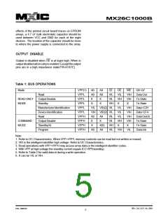
READ MODE
The MX26C1000B has two control functions, both of
which must be logically satisfied in order to obtain data
at the outputs. Chip Enable (CE) is the power control
and should be used for device selection. Output Enable
(OE) is the output control and should be used to gate
datatotheoutputpins, independentofdeviceselection.
Assuming that addresses are stable, address access
time(tACC)isequaltothedelayfromCEtooutput(tCE).
DataisavailableattheoutputstOEafterthefallingedge
of OE, assuming that CE has been LOW and addresses
have been stable for at least tACC - tOE.
PROGRAM VERIFY MODE
Verificationshouldbeperformedontheprogrammedbits
to determine that they were correctly programmed.
Verification should be performed with OE and CE, at
VIL, WE at VIH, and VPP at its programming voltage.
STANDBY MODE
The MX26C1000B has a CMOS standby mode which
reduces the maximum VCC current to 100 uA. It is
placed in CMOS standby when CE is at VCC ±0.3 V.
The MX26C1000B also has a TTL-standby mode which
reduces the maximum VCC current to 1.5 mA. It is
placed in TTL-standby when CE is at VIH. When in
standby mode, the outputs are in a high-impedance
state, independent of the OE input.
ERASE VERIFY MODE
Verification should be performed on the erased chip to
determine that the whole chip(all bits) was correctly
erased. Verification should be performed with OE and
CE at VIL, WE at VIH, and VCC = 5V, VPP = 12.5V
AUTO IDENTIFY MODE
SYSTEM CONSIDERATIONS
Theautoidentifymodeallowsthereadingoutofabinary
code from MTP EPROM that will identify its
manufacturer and device type. This mode is intended
for use by programming equipment for the purpose of
automatically matching the device to be programmed
with its corresponding programming algorithm. This
modeisfunctionalinthe25°C±5°Cambienttemperature
range that is required when programming the
MX26C1000B.
During the switch between active and standby
conditions, transient current peaks are produced on the
rising and falling edges of Chip Enable. The magnitude
of these transient current peaks is dependent on the
outputcapacitanceloadingofthedevice. Ataminimum,
a0.1uFceramiccapacitor(highfrequency,lowinherent
inductance) should be used on each device between
VCCandGNDtominimizetransienteffects. Inaddition,
to overcome the voltage drop caused by the inductive
Toactivatethismode,theprogrammingequipmentmust
REV. 0.6, OCT. 04, 2001
P/N: PM0767
4

 Macronix [ MACRONIX INTERNATIONAL ]