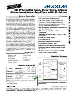
5V, Differential Input, DirectDrive, 130mW
Stereo Headphone Amplifiers with Shutdown
ABSOLUTE MAXIMUM RATINGS
PGND to SGND .....................................................-0.3V to +0.3V
PV to SV ............................................................................0V
SS SS
PV
and SV
to PGND or SGND.........................-0.3V to +6V
Output Short Circuit to GND.......................................Continuous
DD
SS
DD
PV and SV to PGND..........................................+0.3V to -6V
IN_ to SGND ................................(SV - 0.3V) to (SV
OUT_ to PGND ......................................................-3.0V to +3.0V
SHDN to SGND..........................(SGND - 0.3V) to (SV
C1P to PGND ...........................................-0.3V to (PV
C1N to PGND............................................(SV - 0.3V) to +0.3V
PV
Continuous Power Dissipation (T = +70°C)
SS
A
+ 0.3V)
16-Pin Thin QFN (derate 14.7mW/°C above +70°C)....1176mW
16-Pin TSSOP (derate 9.4mW/°C above +70°C) .........755mW
Junction Temperature......................................................+150°C
Operating Temperature Range............................-40°C to +85°C
Storage Temperature Range .............................-65°C to +150°C
Lead Temperature (soldering, 10s) .................................+300°C
SS
DD
+ 0.3V)
+ 0.3V)
DD
DD
SS
to SV ...........................................................................0V
DD
DD
Stresses beyond those listed under “Absolute Maximum Ratings” may cause permanent damage to the device. These are stress ratings only, and functional
operation of the device at these or any other conditions beyond those indicated in the operational sections of the specifications is not implied. Exposure to
absolute maximum rating conditions for extended periods may affect device reliability.
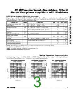
ELECTRICAL CHARACTERISTICS
(PV
= SV
= +5V, PGND = SGND = 0V, SHDN = SV , C1 = C2 = 1µF, R = ∞, resistive load referenced to ground, for
DD
DD DD L
MAX9722A gain = -1V/V (R = R = 10kΩ), for MAX9722B gain = -2V/V (internally set), T = -40°C to +85°C, unless otherwise noted.
Typical values are at T = +25°C, unless otherwise noted.) (Note 1)
IN
F
A
A
PARAMETER
GENERAL
SYMBOL
CONDITIONS
MIN
TYP
MAX UNITS
Supply Voltage Range
Quiescent Supply Current
Shutdown Supply Current
SHDN Input Logic High
SHDN Input Logic Low
SHDN Input Leakage Current
SHDN to Full Operation Time
AMPLIFIERS
V
Guaranteed by PSRR test
2.4
5.5
13
2
V
mA
µA
V
DD
I
R = ∞
L
5.5
0.1
DD
I
SHDN = SGND
SHDN
V
2
IH
V
0.8
+1
V
IL
-1
+0.05
80
µA
µs
t
SON
Voltage Gain
A
MAX9722B (Note 2)
-1.98
-2
2
-2.02
V/V
%
V
Gain Matching
MAX9722B, between the right and left channels
Between IN_+ and IN_-, AC-coupled (MAX9722A)
Between IN_+ and IN_-, AC-coupled (MAX9722B)
IN_+ and IN_-
0.5
1.5
50
2.5
5
Input Offset Voltage
V
mV
IS
Input Bias Current
Input Impedance
I
nA
BIAS
R
MAX9722B, measured at IN_
10
14.4
20
kΩ
IN
Input Common-Mode Voltage
Range
V
-0.5
+0.7
V
CM
Common-Mode Rejection Ratio
CMRR
PSRR
Input referred, MAX9722A, T = +25°C
-60
-80
-70
-90
-80
-50
70
dB
A
DC, V
= 2.4V to 5.5V, input referred
DD
Power-Supply Rejection Ratio
(Note 3)
dB
f = 217Hz, 100mV
f = 10kHz, 100mV
ripple, input referred
ripple, input referred
P-P
P-P
R = 16Ω, THD+N = 1%, T = +25°C
60
L
A
Output Power
P
V
mW
OUT
OUT
R = 32Ω, THD+N = 1%, T = +25°C
130
2
L
A
Output Voltage
R = 1kΩ
L
V
RMS
Output Impedance in Shutdown
10
kΩ
2
_______________________________________________________________________________________

 MAXIM [ MAXIM INTEGRATED PRODUCTS ]