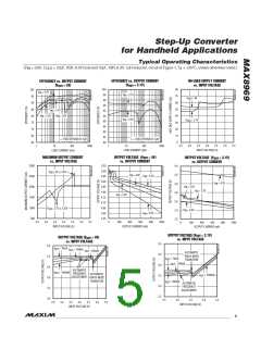
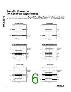
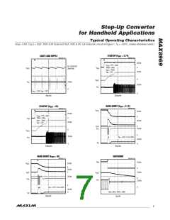
Step-Up Converter
for Handheld Applications
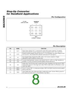
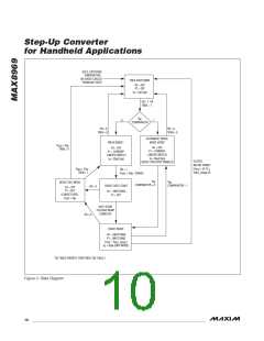
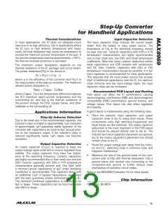
OUT_
C
OUT
22µF
MAX8969
IN
REFERENCE
C
IN
4.7µF
RAMP
IN
GENERATOR
ATM
COMPARATOR
IN
P1
N1
TRUE
SHUTDOWN
ATM
TRACK
PWM
LOGIC
0.95 x
OUT_TARGET
V
CONTROL
LOGIC
ENABLE
TREN
EN
CURRENT
LIMIT
GND_
LX_
L1
1µH
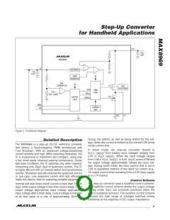
Figure 1. Functional Diagram
During this period, as well as being limited by the volt-
age, ramp rate current is limited by the normal 2.6A boost
mode current limit.
Detailed Description
The MAX8969 is a step-up DC-DC switching converter
that utilizes a fixed-frequency PWM architecture with
True Shutdown. With an advanced voltage-positioning
control scheme and high 3MHz switching frequency, the
IC is inexpensive to implement and compact, using only
a few small easily obtained external components. Under
light-load conditions, the IC switches only when needed,
consuming only 45FA (typ) of quiescent current. The IC
is highly efficient with an internal switch and synchronous
rectifier. Shutdown typically reduces the quiescent current
to 1FA (typ). Low quiescent current and high efficiency
make this device ideal for powering portable equipment.
In boost mode, the step-up converter boosts to
V
from battery input voltages ranging from
OUT_TARGET
2.5V to V . When the input voltage ranges
OUT_TARGET
from 0.95 x V
to 5.5V, the IC enters ATM and
OUT_TARGET
the output voltage approximately follows the input volt-
age. During boost mode, the input current limit is set to
2.6A to guarantee delivery of the rated out current (e.g.,
1A output current when boosting from a 2.5V input supply
to a 3.7V output).
Control Scheme
The step-up converter uses a load/line control scheme.
The load/line control scheme allows the output voltage
to sag under load, but prevents overshoot when the
load is suddenly removed. The load/line control scheme
reduces the total range of voltages reached during
transients at the expense of DC output impedance.
Internal soft-start limits inrush current to less than 720mA
(typ), while output voltage is less than input voltage. Once
output voltage approaches input voltage approaches
input voltage after a brief delay, output voltage is boosted
to its final value at a rate of approximately 25mV/µs.
_______________________________________________________________________________________
9

 MAXIM [ MAXIM INTEGRATED PRODUCTS ]