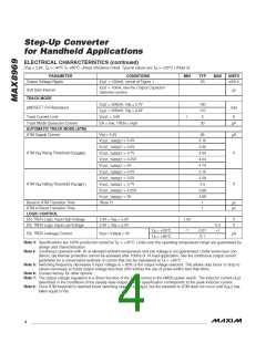
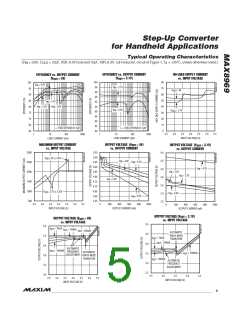
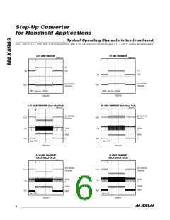
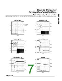
Step-Up Converter
for Handheld Applications
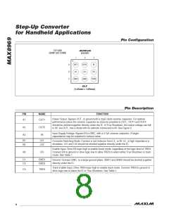
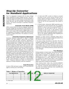
Pin Configuration
TOP VIEW
(BUMP SIDE DOWN)
MAX8969
1
2
3
IN
+
A
B
C
OUT1
LX1
OUT2
LX2
EN
GND1
GND2
TREN
WLP
(1.25mm × 1.25mm)
Pin Description
PIN
NAME
FUNCTION
Power Output. Bypass OUT_ to ground with a 22FF rated ceramic capacitor. For optimal
performance place the ceramic capacitor as close as possible to OUT_. OUT1 and OUT2
should be shorted together directly under the IC. In True Shutdown, the output voltage can fall
to 0V, but OUT_ has a diode with its cathode connected to IN. See Figure 3.
A1
OUT1
A2
A3
OUT2
IN
Input Supply Voltage. Bypass IN to GND_ with a 4.7FF ceramic capacitor. A larger
capacitance may be required to reduce noise.
B1
B2
LX1
LX2
Converter Switching Node. Connect a 1FH inductor from LX_ to IN. LX_ is high impedance in
shutdown. LX1 and LX2 should be shorted together directly under the IC.
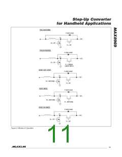
Enable Input. Drive EN logic-high to enable boost mode, regardless of the logic level of TREN.
Connect EN to ground or drive logic-low to allow TREN to select either True Shutdown or track
mode. See Table 1.
B3
EN
C1
C2
GND1
GND2
Ground. Connect GND_ to a large ground plane. GND1 and GND2 should be shorted together
directly under the IC.
Track Enable Input. Drive TREN logic-high to enable track mode. Connect TREN to ground or
drive logic-low to place the IC in True Shutdown. See Table 1.
C3
TREN
8
______________________________________________________________________________________

 MAXIM [ MAXIM INTEGRATED PRODUCTS ]