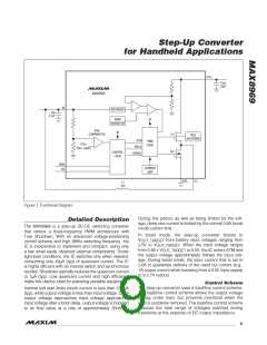
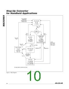
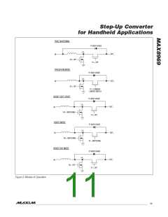
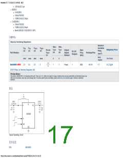
Step-Up Converter
for Handheld Applications
Thermal Considerations
Input Capacitor Selection
IN
drawn from the battery or input power source. The
impedance of C at the switching frequency should
In most applications, the IC does not dissipate much
heat due to its high efficiency. But in applications where
the IC runs at high ambient temperature with heavy
loads, the heat dissipated may cause the temperature to
exceed the maximum junction temperature of the part. If
the junction temperature reaches approximately +165NC,
the thermal overload protection is activated.
The input capacitor (C ) reduces the current peaks
IN
be kept very low. Ceramic capacitors with X5R or X7R
temperature characteristics are highly recommended
due to their small size, low ESR, and small temperature
coefficients. Note that some ceramic dielectrics exhibit
large capacitance and ESR variation with temperature
and DC bias. Ceramic capacitors with Z5U or Y5V
temperature characteristics should be avoided. A 4.7FF
input capacitor is recommended for most applications.
This assumes that the input power source has at least
22FF of additional capacitance near the IC. For optimum
noise immunity and low input-voltage ripple, the input
capacitor value can be increased.
The maximum power dissipation depends on the
thermal resistance of the IC package and circuit board.
The power dissipated (P ) in the device is:
D
P
= P
x (1/E - 1)
D
OUT
where E is the efficiency of the converter and P
is
OUT
the output power of the step-up converter. The maximum
allowed power dissipation is:
P
= (T
- T )/B
MAX
JMAX A JA
Recommended PCB Layout and Routing
Poor layout can affect the IC performance, causing
electromagnetic interference (EMI) and electromagnetic
compatibility (EMC) performance, ground bounce, and
voltage losses. Poor layout can also affect regulation
and stability.
where (T
- T ) is the temperature difference between
A
the IC’s maximum rated junction temperature and the
surrounding air, and B is the thermal resistance of
the junction through the PCB, copper traces, and other
materials to the surrounding air.
JMAX
JA
A good layout is implemented using the following rules:
Applications Information
•ꢀ Place the inductor, input capacitor, and output
capacitor close to the IC using short traces. These
components carry high switching frequencies and
large traces act like antennas. The output capacitor
placement is the most important in the PCB layout
and should be placed directly next to the IC. The
inductor and input capacitor placement are second-
ary to the output capacitor’s placement but should
remain close to the IC.
Step-Up Inductor Selection
Due to the small size of the recommended capacitor, the
inductor’s value is limited to approximately 1FH. Inductors
of approximately 1FH guarantee stable operation of the
converter with capacitance as small as 8FF (actual) pres-
ent on the converter’s output. If the inductor’s value is
reduced significantly below 1FH, ripple can become
excessive.
Output Capacitor Selection
•ꢀ Route the output voltage path away from the induc-
tor and LX_ switching node to minimize noise and
magnetic interference.
An output capacitor (C
) is required to keep the
OUT
output-voltage ripple small and to ensure regulation loop
stability. The output capacitor must have low imped-
ance at the switching frequency. Ceramic capacitors
are highly recommended due to their small size and low
ESR. Ceramic capacitors with X5R or X7R temperature
characteristics generally perform well. One 22FF (with
a minimum actual capacitance of 6FF under operating
conditions) is recommended. This capacitor along with
an additional 10FF of bypass capacitance, associated
with the load, guarantee proper performance of the IC.
The minimum combined capacitance is required to be
8FF or larger. These capacitors can be found with case
size 0603 or larger.
•ꢀ Maximize the size of the ground metal on the com-
ponent side to help with thermal dissipation. Use a
ground plane with several vias connecting to the
component-side ground to further reduce noise
interference on sensitive circuit nodes.
Refer to the MAX8969 Evaluation Kit for more details.
Chip Information
PROCESS: BiCMOS
______________________________________________________________________________________ 13

 MAXIM [ MAXIM INTEGRATED PRODUCTS ]