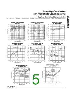
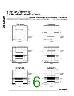
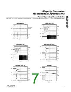
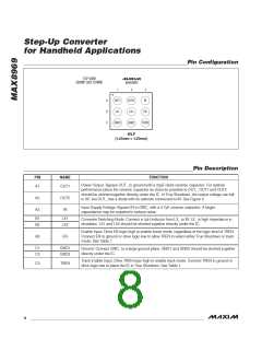
Step-Up Converter
for Handheld Applications
ELECTRICAL CHARACTERISTICS (continued)
(V = 2.6V, T = -40NC to +85NC, unless otherwise noted. Typical values are T = +25NC.) (Note 3)
IN
A
A
PARAMETER
CONDITIONS
MIN
TYP
MAX
UNITS
mV
Output Voltage Ripple
Soft-Start Interval
TRACK MODE
I
I
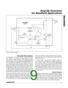
= 150mA, circuit of Figure 1
20
OUT
P-P
= 10mA, see the Output Capacitor
Selection section
OUT
Fs
I
I
= 500mA, V = 2.7V
130
110
2
OUT
IN
pMOSFET On-Resistance
mI
= 500mA, V = 3.2V
IN
OUT
Track Current Limit
V
= 3.6V
1
A
OUT
Track Mode Quiescent Current
AUTOMATIC TRACK MODE (ATM)
ATM Supply Current
EN = low, TREN = high
30
FA
V
V
V
V
V
V
V
V
V
V
V
= 5.4V
65
FA
IN
_
= 3.3V
= 3.5V
= 3.7V
= 4.25V
= 5V
3.15
3.35
3.55
4.04
4.74
3.10
3.29
3.5
OUT TARGET
_
OUT TARGET
ATM V Rising Threshold (V
_
OUT TARGET
V
IN
ATMRT)
_
OUT TARGET
_
OUT TARGET
_
= 3.3V
= 3.5V
= 3.7V
= 4.25V
= 5V
OUT TARGET
_
OUT TARGET
ATM V Falling Threshold (V
IN
_
OUT TARGET
V
ATMFT)
_
3.99
OUT TARGET
_
4.69
1
OUT TARGET
Boost to ATM Transition Time
ATM to Boost Transition Time
LOGIC CONTROL
(Note 7)
Fs
Fs
1
EN, TREN Logic Input High Voltage
EN, TREN Logic Input Low Voltage
2.3V < V < 5.5V
1.05
-1
V
V
IN
2.3V < V < 5.5V
0.4
+1
IN
T
T
= +25NC
= +85NC
0.01
0.1
A
A
EN, TREN Leakage Current
V
= V
= 0V
FA
EN
TREN
Note 3: Specifications are 100% production tested at T = +25°C. Limits over the operating temperature range are guaranteed by
A
design and characterization.
Note 4: Continuous operation with 1A at elevated ambient temperature and low voltage is not guaranteed. Under worst-case con-
ditions, die thermal protection cannot be activated after 100ms of 1A load application. See the continuous output current
parameter for a conservative estimate of current that can be maintained at T = +85°C.
A
Note 5: Switching frequency decreases if input voltage is > 83% of the output voltage selected. This allows duty factor to drop to
values necessary to boost output voltage less than 25% without the use of pulse widths less than 60ns.
Note 6: Contact factory for other options.
Note 7: The output voltage regulation is a direct function of the peak current in the nMOS power switch. The inductor current (I
)
LX
described in the conditions of the steady-state output voltage specification corresponds to the peak inductor current.
Note 8: Once ATM threshold is reached boost switching stops in 1µs (typ), but the transition to ATM does not occur until V
has
OUT
fallen equal to V
.
IN
4
______________________________________________________________________________________

 MAXIM [ MAXIM INTEGRATED PRODUCTS ]