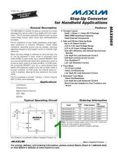
Step-Up Converter
for Handheld Applications
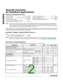
ABSOLUTE MAXIMUM RATINGS
IN, OUT_ to GND_................................................-0.3V to +6.0V
Operating Temperature Range.......................... -40NC to +85NC
EN, TREN to GND_ ............ -0.3V to lower of (V + 0.3V) or 6V
Junction Temperature .....................................................+150NC
Storage Temperature Range............................ -65NC to +150NC
Soldering Temperature (reflow) (Note 1) ........................+260NC
IN
Total LX_ Current...........................................................3.2A
RMS
OUT_ Short Circuit to GND_ .....................................Continuous
Continuous Power Dissipation (T = +70NC)
A
WLP (derate 12mW/NC above +70NC).........................960mW
Note 1: This device is constructed using a unique set of packaging techniques that impose a limit on the thermal profile that the
device can be exposed to during board level solder attach and rework. This limit permits only the use of the solder pro-
files recommended in the industry-standard specification JEDEC 020A, paragraph 7.6, Table 3 for IR/VPR and Convection
reflow. Preheating is required. Hand or wave soldering is not allowed.
Stresses beyond those listed under “Absolute Maximum Ratings” may cause permanent damage to the device. These are stress ratings only, and functional
operation of the device at these or any other conditions beyond those indicated in the operational sections of the specifications is not implied. Exposure to absolute
maximum rating conditions for extended periods may affect device reliability.
PACKAGE THERMAL CHARACTERISTICS (Note 2)
WLP
Junction-to-Ambient Thermal Resistance (B ) ..........83NC/W
JA
Junction-to-Case Thermal Resistance (B )...............50NC/W
JC
Note 2: Package thermal resistances were obtained using the method described in JEDEC specification JESD51-7, using a four-
layer board. For detailed information on package thermal considerations, refer to www.maxim-ic.com/thermal-tutorial.
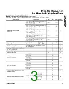
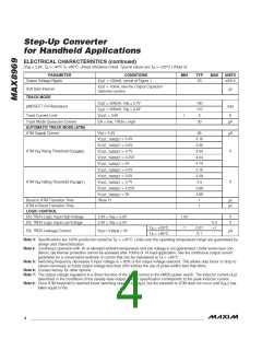
ELECTRICAL CHARACTERISTICS
(V = 2.6V, T = -40NC to +85NC, unless otherwise noted. Typical values are T = +25NC.) (Note 3)
IN
A
A
PARAMETER
CONDITIONS
MIN
TYP
MAX
UNITS
Operating Input Voltage Range
Minimum Startup Voltage
2.5
5.5
V
V
2.3
2.2
Undervoltage Lockout Threshold (UVLO)
V
falling, 75mV hysteresis
2.1
2.3
5
V
IN
T
T
= +25NC
0.8
1
V
V
= V
= V = 0V,
OUT
A
A
EN
TREN
Shutdown Supply Current
FA
NC
= 4.8V
IN
= +85NC
Thermal Shutdown
BOOST MODE
T
rising, 20NC hysteresis
+165
A
Peak Output Current
V
> 2.5V (Note 4)
1
A
IN
V
OUT
V
OUT
V
OUT
V
OUT
V
OUT
V
OUT
= 3.3V
= 3.5V
= 3.7V
= 4.25V
= 4.7V
= 5.0V
0.9
0.8
0.7
0.7
0.7
0.7
V
load
> 2.5V, pulse
IN
Continuous Output Current
A
Switching Frequency
(Note 4)
3
MHz
V
No load, V
No load, V
No load, V
No load, V
No load, V
_
= 3.3V
= 3.5V
= 3.7V
3.175
3.40
3.64
4.10
4.85
3.30
3.50
3.75
4.25
5.00
3.40
3.60
3.85
4.35
5.10
OUT TARGET
_
OUT TARGET
_
Output Voltage Accuracy
OUT TARGET
_
= 4.25V
= 5V
OUT TARGET
_
OUT TARGET
2
______________________________________________________________________________________

 MAXIM [ MAXIM INTEGRATED PRODUCTS ]