Smallest TEC Power Drivers for
Optical Modules
Detailed Description
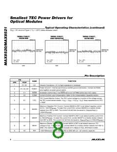
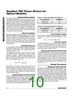
Table 1. TEC Connection for Figure 1
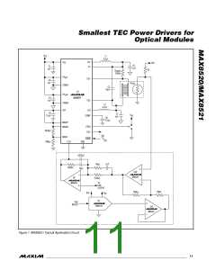
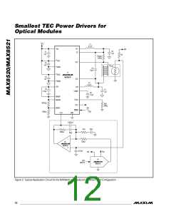
The MAX8520/MAX8521 TEC drivers consist of two
switching buck regulators that operate together to directly
control the TEC current. This configuration creates a
differential voltage across the TEC, allowing bidirectional
TEC current for controlled cooling and heating. Controlled
cooling and heating allow accurate TEC temperature con-
trol to within 0.01°C. The voltage at CTLI directly sets
the TEC current. An external thermal- control loop is typi-
cally used to drive CTLI. Figures 1 and 2 show examples
of the thermal control-loop circuit.
TEC CONNECTION
Heating mode
THERMISTOR
PTC
Cooling mode
NTC
Table 2. TEC Connection for Figure 2
TEC CONNECTION
Heating mode
THERMISTOR
NTC
Cooling mode
PTC
Ripple Cancellation
Switching regulators like those used in the MAX8520/
MAX8521 inherently create ripple voltage on the output.
The dual regulators in the MAX8520/MAX8521 switch in
phase and provide complementary in-phase duty
cycles so ripple waveforms at the TEC are greatly
reduced. This feature suppresses ripple currents and
electrical noise at the TEC to prevent interference with
the laser diode.
Current Monitor Output
ITEC provides a voltage output proportional to the TEC
current (I
details:
). See the Functional Diagram for more
TEC
V
ITEC
= 1.5V +(8 ✕ (VOS1-VCS))
Reference Output
The MAX8520/MAX8521 include an on-chip voltage ref-
erence. The 1.50V reference is accurate to 1% over
temperature. Bypass REF with 0.1µF to GND. REF can
be used to bias an external thermistor for temperature
sensing as shown in Figures 1 and 2.
Switching Frequency
For the MAX8521, FREQ sets the switching frequency of
the internal oscillator. With FREQ = GND, the oscillator
frequency is set to 500kHz. The oscillator frequency is
Thermal and Fault-Current Protection
The MAX8520/MAX8521 provide fault-current protection
in either FET by turning off both high-side and low-side
FETs when the peak current exceeds 3A in either FET. In
addition, thermal-overload protection limits the total
power dissipation in the chip. When the device’s die junc-
tion temperature exceeds +165°C, an on-chip thermal
sensor shuts down the device. The thermal sensor turns
the device on again after the junction temperature cools
down by 15°C.
1MHz when FREQ = V
.
DD
For the MAX8520, connect a resistor (R
in Figure 2)
EXT
from FREQ to GND. Choose R
= 60kΩ for 1MHz
EXT
operation, and R
= 150kΩ for 500kHz operation. For
EXT
any intermediary frequency between 500kHz and
1MHz, use the following equation to find the value of
R
value needed for V
= 5V:
EXT
DD
1
fs
1
3
R
= 90 ×
−
EXT
Design Procedures
where R
is the resistance given in kΩ, and fs is the
EXT
Duty-Cycle Range Selection
By design, the MAX8520/MAX8521 are capable of oper-
ating from 0% to 100% duty cycle, allowing both LX out-
puts to enter dropout. However, as the LX pulse width
narrows, accurate duty-cycle control becomes difficult.
This can result in a low-frequency noise appearing at the
TEC output (typically in the 20kHz to 50kHz range). While
this noise is typically filtered out by the low thermal-loop
bandwidth, for best results, operate the PWM with a pulse
width greater than 200ns. For a 500kHz application, the
recommended duty-cycle range is from 10% to 90%. For
a 1MHz application, it is from 20% to 80%.
desired frequency given in MHz. Note that for V
<
DD
5V, the frequency is reduced slightly, to the extent of
about 7% when V reaches 3V. This should be taken
DD
into consideration when selecting the value for R
a known supply voltage.
at
EXT
Voltage and Current-Limit Setting
Both the MAX8520 and MAX8521 provide control of the
maximum differential TEC voltage. Applying a voltage
to MAXV limits the maximum voltage across the TEC.
The voltage at MAXIP and MAXIN sets the maximum
positive and negative current through the TEC. These
current limits can be independently controlled.
10 ______________________________________________________________________________________

 MAXIM [ MAXIM INTEGRATED PRODUCTS ]