Smallest TEC Power Drivers for
Optical Modules
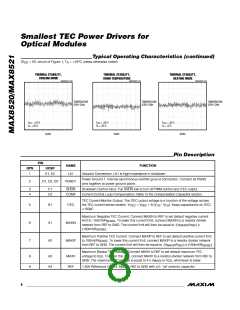
Pin Description (continued)
PIN
NAME
FUNCTION
QFN
UCSP
TEC Current-Control Input. Sets TEC current. Center point is 1.50V (no TEC current). The
current is given by:
10
A5
CTLI
GND
I
= (V
- V ) / R
= (V
- 1.50) / (10 x R
). When (V
- V
REF
) > 0,
TEC
OS1
CS
SENSE
CTLI
SENSE
CTLI
then V
> V
> V
.
CS
OS2
OS1
11
12
A6
B6
Analog Ground. Start connect to PGND at underside exposed pad for QFN package.
Analog Supply Voltage Input. Bypass V to GND with a 1µF ceramic capacitor.
V
DD
DD
For MAX8520: Analog FREQ Set Pin (see the Switching Frequency section).
For MAX8521: Digital FREQ Selection Pin. Tie to V for 1MHz operation, tie to GND for
DD
500kHz operation. The PWM oscillator can synchronize to FREQ by switching at FREQ
between 700kHz and 1.2MHz.
13
C5
FREQ
Power Ground 2. Internal synchronous rectifier ground connection. Connect all PGND
pins together at the power ground plane.
14
D4, D5, D6
PGND2
LX2
15
16
E5, E6
F5, F6
Inductor Connection. LX2 is high impedance in shutdown.
PV
DD
2
Power Input 2. Connect all PV
inputs together at the V
power plane.
DD
DD
Current-Sense Input. The current through the TEC is monitored between CS and OS1. The
maximum TEC current is given by 150mV/R and is bipolar.
17
18
F4
CS
SENSE
Output Sense 2. OS2 senses one side of the differential TEC voltage. OS2 is a sense
point, not a power output. OS2 discharges to ground in shutdown.
C6
OS2
OS1
Output Sense 1. OS1 senses one side of the differential TEC voltage. OS1 is a sense
point, not a power output. OS1 discharges to ground in shutdown.
19
20
F3
F1, F2
PV
DD
1
Power Input 1. Connect all PV
inputs together at the V
power plane.
DD
DD
B2, B5,
C3, C4
Ground. Additional ground pads aid in heat dissipation. Short to either GND or PGND
plane.
GND2
N.C.
B3, B4
E3, E4
No Connect. Connect no-connect pads to GND2 to aid in heat dissipation.
_______________________________________________________________________________________
9

 MAXIM [ MAXIM INTEGRATED PRODUCTS ]