S e ria lly In t e rfa c e d , 8 -Dig it LED Dis p la y Drive rs
CS
OR LOAD
t
CSW
t
CSH
t
CP
t
t
CL
t
CH
t
CSS
LDCK
CLK
t
DH
t
DS
DIN
D15
D14
D1
D0
t
DO
DOUT
9/MAX721
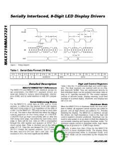
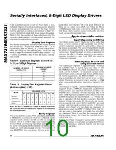
Figure 1. Timing Diagram
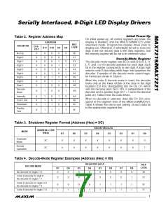
Table 1. Serial-Data Format (16 Bits)
D15
X
D14
X
D13
X
D12
X
D11
D10
D9
D8
D7
D6
D5
D4
MSBDATA
D3
D2
D1
D0
ADDRESS
MSB
LSB
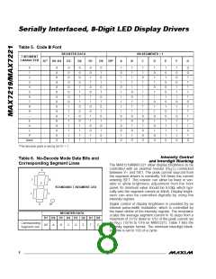
Dig it a n d Co n t ro l Re g is t e rs
_______________De t a ile d De s c rip t io n
Table 2 lists the 14 addressable digit and control regis-
ters. The digit registers are realized with an on-chip,
8x8 dual-port SRAM. They are addressed directly so
that individual digits can be updated and retain data as
long as V+ typically exceeds 2V. The control registers
consist of decode mode, display intensity, scan limit
(number of scanned digits), shutdown, and display test
(all LEDs on).
MAX7 2 1 9 /MAX7 2 2 1 Diffe re n c e s
The MAX7219 and MAX7221 are identical except for
two parameters: the MAX7221 segment drivers are
slew-rate limited to reduce electromagnetic interfer-
ence (EMI), and its serial interface is fully SPI compati-
ble.
S e ria l-Ad d re s s in g Mo d e s
For the MAX7219, serial data at DIN, sent in 16-bit
packets, is shifted into the internal 16-bit shift register
with each rising edge of CLK regardless of the state of
LOAD. For the MAX7221, CS must be low to clock data
in or out. The data is then latched into either the digit or
c ontrol re g is te rs on the ris ing e d g e of LOAD/CS.
LOAD/CS must go high concurrently with or after the
16th rising clock edge, but before the next rising clock
edge or data will be lost. Data at DIN is propagated
through the shift register and appears at DOUT 16.5
clock cycles later. Data is clocked out on the falling
edge of CLK. Data bits are labeled D0–D15 (Table 1).
D8–D11 contain the register address. D0–D7 contain
the data, and D12–D15 are “don’t care” bits. The first
received is D15, the most significant bit (MSB).
S h u t d o w n Mo d e
When the MAX7219 is in shutdown mode, the scan oscil-
lator is halted, all segment current sources are pulled to
ground, and all digit drivers are pulled to V+, thereby
blanking the display. The MAX7221 is identical, except
the drivers are high-impedance. Data in the digit and
control registers remains unaltered. Shutdown can be
used to save power or as an alarm to flash the display by
successively entering and leaving shutdown mode. For
minimum supply current in shutdown mode, logic inputs
should be at ground or V+ (CMOS-logic levels).
Typically, it takes less than 250µs for the MAX7219/
MAX7221 to leave shutdown mode. The display driver
can be programmed while in shutdown mode, and
shutdown mode can be overridden by the display-test
function.
6
_______________________________________________________________________________________

 MAXIM [ MAXIM INTEGRATED PRODUCTS ]