Low-Cost, +5V, Serial-Input,
Voltage-Output, 16-Bit DAC
The external buffer amplifier’s gain-bandwidth product
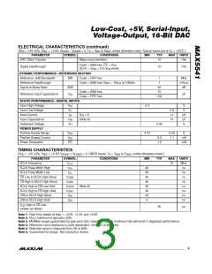
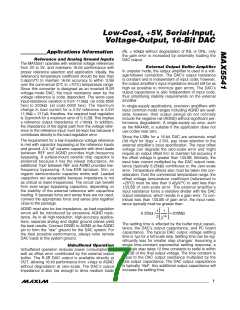
Table 1. Unipolar Code Table
is important because it increases the settling time by
adding another time constant to the output response.
The effective time constant of two cascaded systems,
each with a single time-constant response, is approxi-
mately the root square sum of the two time constants.
The DAC output’s time constant is 1µs / 12 = 83ns,
ignoring the effect of additional capacitance. If the time
constant of an external amplifier with 1MHz bandwidth
is 1 / 2π (1MHz) = 159ns, then the effective time con-
stant of the combined system is:
DAC LATCH CONTENTS
ANALOG OUTPUT, V
OUT
MSB LSB
1111 1111 1111 1111
1000 0000 0000 0000
0000 0000 0000 0001
0000 0000 0000 0000
V
•
(65,535 / 65,536)
(32,768 / 65,536) =
(1 / 65,536)
REF
1/
V
REF
2
V
REF
•
V
REF
•
0V
Power-Supply Bypassing and
Ground Management
2
2
For optimum system performance, use PC boards with
separate analog and digital ground planes. Wire-wrap
boards are not recommended. Connect the two ground
planes together at the low-impedance power-supply
source. Connect DGND and AGND together at the IC.
The best ground connection can be achieved by con-
necting the DAC’s DGND and AGND pins together and
connecting that point to the system analog ground
plane. If the DAC’s DGND is connected to the system
digital ground, digital noise may get through to the
DAC’s analog portion.
96ns + 159ns
=186ns
This suggests that the settling time to within 1/2LSB of
the final output voltage, including the external buffer
amplifier, will be approximately 12 180ns = 2.15µs.
•
Digital Inputs and Interface Logic
The digital interface for the 16-bit DAC is based on a 3-
wire standard that is SPI/QSPI/MICROWIRE compati-
ble. The three digital inputs (CS, DIN, and SCLK) load
the digital input data serially into the DAC.
Bypass V
with a 0.1µF ceramic capacitor connected
DD
DD
All of the digital inputs include Schmitt-trigger buffers to
accept slow-transition interfaces. This means that opto-
couplers can interface directly to the MAX5541 without
additional external logic. The digital inputs are TTL/
CMOS-logic compatible.
between V
and AGND. Mount it with short leads
close to the device. Ferrite beads can also be used to
further isolate the analog and digital power supplies.
Chip Information
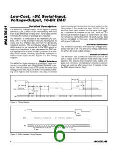
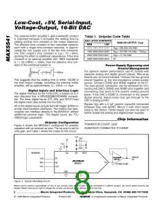
Unipolar Configuration
Figure 3 shows the MAX5541 configured for unipolar
operation with an external op amp. The op amp is set for
unity gain, and Table 1 shows the codes for this circuit.
TRANSISTOR COUNT: 2209
SUBSTRATE CONNECTED TO DGND
+2.5V
+5V
10µF
0.1µF
0.1µF
MC68XXXX
V
REF
(REFS)
DD
UNIPOLAR
OUT
PCS0
MOSI
SCLK
CS
MAX495
OUT
DIN
MAX5541
EXTERNAL OP AMP
SCLK
DGND
AGND_
Figure 3. Typical Operating Circuit
Maxim cannot assume responsibility for use of any circuitry other than circuitry entirely embodied in a Maxim product. No circuit patent licenses are
implied. Maxim reserves the right to change the circuitry and specifications without notice at any time.
8 _____________________Maxim Integrated Products, 120 San Gabriel Drive, Sunnyvale, CA 94086 408-737-7600
© 1999 Maxim Integrated Products
Printed USA
is a registered trademark of Maxim Integrated Products.

 MAXIM [ MAXIM INTEGRATED PRODUCTS ]