Low-Cost, +5V, Serial-Input,
Voltage-Output, 16-Bit DAC
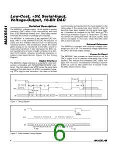
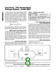
synchronously and latched into the input register on the
Detailed Description
rising edge of the serial-clock input (SCLK). After 16
data bits have been loaded into the serial input regis-
ter, it transfers its contents to the DAC latch on CS’s
low-to-high transition (Figure 2). Note that if CS does
not remain low during the entire 16 SCLK cycles, data
will be corrupted. In this case, reload the DAC latch
with a new 16-bit word.
The MAX5541 voltage-output, 16-bit digital-to-analog
converter (DAC) offers 16-bit monotonicity with less
than 1LSB differential linearity error. Serial-data transfer
minimizes the number of package pins required.
The MAX5541 is composed of two matched DAC sec-
tions, with a 12-bit inverted R-2R DAC forming the 12
LSBs and the 4 MSBs derived from 15 identically
matched resistors. This architecture allows the lowest
glitch energy to be transferred to the DAC output on
major-carry transitions. It also decreases the DAC out-
put impedance by a factor of eight compared to a stan-
dard R-2R ladder, allowing unbuffered operation in
medium-load applications. Figure 1 is the Timing
Diagram.
External Reference
The MAX5541 operates with external voltage refer-
ences from 2V to 3V. The reference voltage determines
the DAC’s full-scale output voltage.
Power-On Reset
The MAX5541 has a power-on reset circuit to set the
DAC’s output to 0V in unipolar mode when V
is first
DD
applied. This ensures that unwanted DAC output volt-
ages will not occur immediately following a system
power-up, such as after power loss. In bipolar mode,
Digital Interface
The MAX5541 digital interface is a standard 3-wire con-
nection compatible with SPI/QSPI/MICROWIRE inter-
faces. The chip-select input (CS) frames the serial data
loading at the data input pin (DIN). Immediately follow-
ing CS’s high-to-low transition, the data is shifted
the DAC output is set to -V
.
REF
t
CSH1
CS
t
CSHO
t
CSS1
t
t
t
CL
CSSO
CH
SCLK
DIN
t
DH
t
DS
D15
D14
D0
Figure 1. Timing Diagram
CS
DAC
UPDATED
SCLK
DIN
D15 D14 D13 D12 D11 D10 D9 D8
MSB
D7 D6 D5 D4 D3 D2 D1 D0
LSB
Figure 2. 3-Wire Interface Timing Diagram
6
_______________________________________________________________________________________

 MAXIM [ MAXIM INTEGRATED PRODUCTS ]