Lo w -P o w e r, Du a l, 1 2 -Bit Vo lt a g e -Ou t p u t DACs
w it h S e ria l In t e rfa c e
ABSOLUTE MAXIMUM RATINGS
V
to AGND............................................................-0.3V to +6V
to DGND ...........................................................-0.3V to +6V
Continuous Power Dissipation (T = +70°C)
A
DD
V
Plastic DIP (derate 10.5mW/°C above +70°C) ...........842mW
QSOP (derate 8.30mW/°C above +70°C)...................667mW
CERDIP (derate 10.00mW/°C above +70°C)..............800mW
Operating Temperature Ranges
DD
AGND to DGND..................................................................±0.3V
OSA, OSB to AGND........................(AGND - 4V) to (V + 0.3V)
REF_, OUT_ to AGND.................................-0.3V to (V + 0.3V)
DD
DD
Digital Inputs (SCLK, DIN, CS, CL, PDL)
to DGND............................................................(-0.3V to +6V)
Digital Outputs (DOUT, UPO)
MAX515_ _C_ E .................................................0°C to +70°C
MAX515_ _E_ E ..............................................-40C° to +85°C
MAX515_ _MJE.............................................-55°C to +125°C
Storage Temperature Range .............................-65°C to +150°C
Lead Temperature (soldering, 10sec) .............................+300°C
to DGND................................................-0.3V to (V + 0.3V)
DD
Maximum Current into Any Pin .........................................±20mA
Stresses beyond those listed under “Absolute Maximum Ratings” may cause permanent damage to the device. These are stress ratings only, and functional
operation of the device at these or any other conditions beyond those indicated in the operational sections of the specifications is not implied. Exposure to
absolute maximum rating conditions for extended periods may affect device reliability.
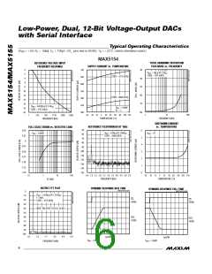
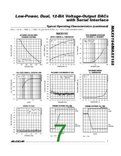
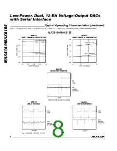
ELECTRICAL CHARACTERISTICS—MAX5154
(V = +5V ±10%, V
= V
= 2.048V, R = 10kΩ, C = 100pF, T = T
to T , unless otherwise noted. Typical values are
MAX
DD
REFA
REFB
L
L
A
MIN
at T = +25°C (OS_ tied to AGND for a gain of +2V/V).)
A
PARAMETER
STATIC PERFORMANCE
Resolution
SYMBOL
CONDITIONS
MIN
TYP
MAX
UNITS
4/MAX15
12
Bits
MAX5154A
MAX5154B
±1/2
±1
Integral Nonlinearity
INL
(Note 1)
LSB
Differential Nonlinearity
Offset Error
DNL
Guaranteed monotonic
Code = 6
±1
LSB
mV
V
os
±6
Offset Tempco
Gain Error
TCV
Normalized to 2.048V
4
-0.2
4
ppm/°C
LSB
os
±3
Gain-Error Tempco
Normalized to 2.048V
ppm/°C
V
Power-Supply
DD
PSRR
REF
4.5V ≤ V ≤ 5.5V
20
260
µV/V
DD
Rejection Ratio
REFERENCE INPUT
Reference Input Range
Reference Input Resistance
0
V
- 1.4
V
DD
R
Minimum with code 1554 hex
Input code = 1FFE hex,
14
20
kΩ
REF
MULTIPLYING-MODE PERFORMANCE
Reference 3dB Bandwidth
300
-82
75
kHz
dB
V
REF_
= 0.67Vp-p at 2.5V
DC
Input code = 0000 hex,
= (V - 1.4Vp-p) at 1kHz
Reference Feedthrough
Signal-to-Noise plus
V
REF_
DD
Input code = 1FFE hex,
V = 1Vp-p at 1.25V , f = 25kHz
REF_
SINAD
dB
Distortion Ratio
DC
DIGITAL INPUTS
Input High Voltage
Input Low Voltage
Input Hysteresis
V
3
V
V
CL, PDL, CS, DIN, SCLK
CL, PDL, CS, DIN, SCLK
IH
V
IL
0.8
±1
V
HYS
200
0.001
8
mV
µA
pF
Input Leakage Current
Input Capacitance
I
IN
V
= 0V to V
IN DD
C
IN
2
_______________________________________________________________________________________

 MAXIM [ MAXIM INTEGRATED PRODUCTS ]