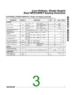
Low-Voltage, Single-Supply
Dual SPST/SPDT Analog Switches
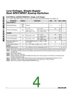
Pin Description
Analog Switch 1—Normally Open
1
1
—
—
1
1
—
—
NO1
PIN
MAX4541
MAX4542
MAX4543
MAX4544
NAME
FUNCTION
DIP/SO/
DIP/SO/
µMAX/
QFN
DIP/SO/
µMAX/
QFN
DIP/SO/
µMAX/
QFN
SOT23-8
SOT23-8
SOT23-8
SOT23-6
µMAX/
QFN
1
1
8
—
—
8
1
1
8
—
—
—
4
—
—
—
3
NO1
COM1
IN2
Analog Switch 1—Normally Open
Analog Switch 1—Common
Digital Control Input 2
2
2
2
3
3
3
3
3
3
4
6
4
6
4
6
GND
NO2
COM2
IN1
Ground—Negative Supply Input
Analog Switch 2—Normally Open
Analog Switch 2—Common
Digital Control Input 1
5
5
—
6
—
4
—
6
—
4
—
—
—
8
—
—
—
2
6
4
7
7
7
7
7
7
8
2
8
2
8
2
V+
Positive Supply Voltage Input
Analog Switch 1—Normally Closed
Analog Switch 2—Normally Closed
Analog Switch—Normally Open
Analog Switch—Common
—
—
—
—
—
—
—
—
—
—
—
—
—
—
1
1
—
5
—
5
—
—
1
—
—
6
NC1
NC2
NO
5
5
—
—
—
—
—
—
—
—
—
—
—
—
—
—
—
—
—
—
—
—
2
5
COM
NC
3
4
Analog Switch—Normally Closed
Not Connected (open circuit)
Digital Control Input
5, 6
7
—
1
N.C.
IN
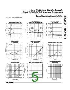
Applications Information
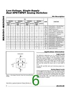
POSITIVE SUPPLY
D1
Logic Levels
The MAX4541–MAX4544 are TTL compatible when
powered from a single +5V supply. When powered
from other supply voltages, TTL compatibility is guar-
anteed and the logic inputs can be driven Rail-to-Rail®.
For example, with a +12V supply, IN1 and IN2 can be
driven low to 0 and high to 12V. With a +3.3V supply,
IN1 and IN2 should be driven low to 0 and high to
3.3V.
V+
NO
COM
V
g
Driving IN1 and IN2 rail-to-rail minimizes power con-
sumption.
GND
Analog Signal Levels
Analog signals that range over the entire supply voltage
(V+ to GND) can be switched with very little change in
on-resistance over the entire voltage range (see Typical
Operating Characteristics). All the switches are bidirec-
tional, so the NO_, NC_, and COM_ pins can be used
as either inputs or outputs.
D2
Figure 1. Overvoltage Protection Using Two External Blocking
Diodes
Rail-to-Rail is a registered trademark of Nippon Motorola, Ltd.
6
_______________________________________________________________________________________

 MAXIM [ MAXIM INTEGRATED PRODUCTS ]