Low-Voltage, Single-Supply
Dual SPST/SPDT Analog Switches
ABSOLUTE MAXIMUM RATINGS
Voltage Referenced to GND
QFN (derate 24.4mW/°C above +70°C) ......................1951mW
V+.........................................................................-0.3V to +13V
IN_, COM_, NC_, NO_ (Note 1)..................-0.3V to (V+ + 0.3V)
Continuous Current (any terminal).................................... 10mA
Peak Current, COM_, NO_, NC_
(pulsed at 1ms, 10% duty cycle max)............................ 20mA
ESD per Method 3015.7 ..................................................>2000V
Continuous Power Dissipation
µMAX (derate 4.10mW/°C above +70°C) ......................330mW
Narrow SO (derate 5.88mW/°C above +70°C) ..............471mW
Plastic DIP (derate 9.09mW/°C above +70°C) ..............727mW
Operating Temperature Ranges
MAX454_C_ _ .......................................................0°C to +70°C
MAX454_E_ _.....................................................-40°C to +85°C
Storage Temperature Range.............................-65°C to +150°C
Lead Temperature (soldering, 10s) .................................+300°C
SOT23-6 (derate 7.1mW/°C above +70°C)....................571mW
SOT23-8 (derate 5.3mW/°C above +70°C)....................421mW
Note 1: Signals on NC, NO, COM, or IN exceeding V+ or V- are clamped by internal diodes. Limit forward diode current to maximum
current rating.
Stresses beyond those listed under “Absolute Maximum Ratings” may cause permanent damage to the device. These are stress ratings only, and functional
operation of the device at these or any other conditions beyond those indicated in the operational sections of the specifications is not implied. Exposure to
absolute maximum rating conditions for extended periods may affect device reliability.
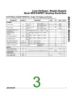
ELECTRICAL CHARACTERISTICS—Single +5V Supply
(V+ = +5V 10%, GND = 0, V
= 2.4V, V
= 0.8V, T = T
to T
, unless otherwise noted.) (Notes 2, 3)
MAX
INH
INL
A
MIN
PARAMETER
SYMBOL
CONDITIONS
MIN
TYP
MAX
UNITS
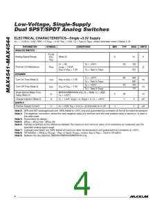
ANALOG SWITCH
V
COM,
Analog Signal Range
On-Resistance
V
V
(Note 4)
0
V+
V
NO,
NC
V+ = 4.5V,
T
T
T
T
T
= +25°C
30
0.8
2
60
75
2
A
A
A
A
A
R
I
= 1.0mA,
Ω
Ω
Ω
COM
ON
= T
to T
MIN
MAX
MAX
MAX
V
NO
or V
= 3.5V
NC
V+ = 5V,
I = 1.0mA,
COM
= +25°C
= T to T
On-Resistance Match
Between Channels (Note 5)
∆R
ON
4
MIN
V
NO
or V
= 3.5V
NC
V+ = 5V;
I = 1.0mA;
= +25°C
= T to T
6
On-Resistance Flatness
(Note 6)
R
FLAT(ON) COM
T
A
T
A
T
A
8
MIN
V
NO
or V = 1V, 2V, 3V
NC
= +25°C
= T
-0.1
-5
0.01
0.1
I
I
V+ = 5.5V;
NO(OFF)
or
NC(OFF)
NO or NC Off-Leakage
Current (Note 7)
V
V
= 1V, 4.5V;
or V
nA
nA
COM
NO
MIN
MAX
C, E
5
= 4.5V, 1V
NC
to T
T
A
= +25°C
-0.1
-5
0.1
5
V+ = 5.5V;
COM Off-Leakage Current
(Note 7)
I
V
V
= 4.5V, 1V;
or V
COM(OFF)
COM
NO
T
A
= T
MIN
MAX
C, E
C, E
= 1V, 4.5V
NC
to T
V+ = 5.5V;
T
A
= +25°C
-0.2
0.2
COM On-Leakage Current
(Note 7)
V
V
= 1V, 4.5V or
or V
COM
NO
I
nA
COM(ON)
T
A
= T
MIN
MAX
= 1V, 4.5V,
NC
-10
10
to T
or floating
2
_______________________________________________________________________________________

 MAXIM [ MAXIM INTEGRATED PRODUCTS ]