Low-Voltage, Single-Supply
Dual SPST/SPDT Analog Switches
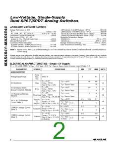
ELECTRICAL CHARACTERISTICS—Single +3.3V Supply
(V+ = +3.0V to +3.6V, GND = 0, V
= 2.4V, V
= 0.8V, T = T
to T
, unless otherwise noted.) (Notes 2, 3)
MAX
INH
INL
A
MIN
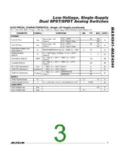
PARAMETER
SYMBOL
CONDITIONS
MIN
TYP
MAX
UNITS
ANALOG SWITCH
V
COM,
Analog Signal Range
V
V
(Note 3)
V+ = 3V,
0
V+
V
NO,
NC
T
T
= +25°C
50
125
275
A
Channel On-Resistance
R
I
= 1.0mA,
Ω
COM
ON
V
NO
or V
= 1.5V
= T
to T
MIN MAX
NC
A
DYNAMIC
T
A
T
A
T
A
T
A
= +25°C
80
50
400
500
125
175
Turn-On Time (Note 3)
t
V
V
or V
or V
= 1.5V
= 1.5V
ns
ns
ON
NO
NC
= T
to T
MIN
MAX
MAX
= +25°C
= T to T
Turn-Off Time (Note 3)
t
OFF
NO
NC
MIN
Break-Before-Make Time
Delay (Note 3)
MAX4543/MAX4544 only, R = 300Ω, C = 35pF,
A
L
L
t
2
30
1
ns
D
T
= +25°C
Charge Injection (Note 3)
SUPPLY
Q
C = 1.0nF, V
= 0, R
= 0, T = +25°C
5
1
pC
L
GEN
GEN
A
Positive Supply Current
I+
V+ = 3.6V, V = 0 or V+, all channels on or off
-1
µA
IN
Note 2: QFN and SOT-packaged parts are 100% tested at +25°C only and guaranteed by correlation at the full hot rated temperature.
Note 3: The algebraic convention, where the most negative value is a minimum and the most positive value a maximum, is used in
this data sheet.
Note 4: Guaranteed by design.
Note 5: ∆R
= ∆R
max - ∆R
min.
ON
ON
ON
Note 6: Flatness is defined as the difference between the maximum and minimum value of on-resistance as measured over the
specified analog signal range.
Note 7: Leakage parameters are 100% tested at maximum rated hot temperature and guaranteed by correlation at +25°C.
Note 8: Off Isolation = 20log
[V
COM
⁄ (V
or V )], V = output, V or V
= input to off switch.
10
NC
NO
COM
NC
NO
Note 9: Between the two switches, MAX4541/MAX4542/MAX4543 only.
4
_______________________________________________________________________________________

 MAXIM [ MAXIM INTEGRATED PRODUCTS ]