Low-Voltage, Single-Supply
Dual SPST/SPDT Analog Switches
Adding protection diodes causes the logic thresholds
to be shifted relative to the power-supply rails. This can
be significant when low supply voltages (+5V or less)
are used. With a +5V supply, TTL compatibility is not
guaranteed when protection diodes are added. Driving
IN1 and IN2 all the way to the supply rails (i.e., to a
diode drop higher than the V+ pin, or to a diode drop
lower than the GND pin) is always acceptable.
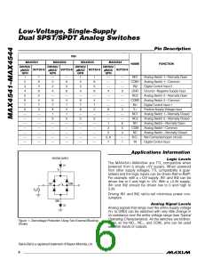
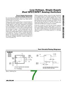
Power-Supply Sequencing
and Overvoltage Protection
Do not exceed the absolute maximum ratings because
stresses beyond the listed ratings may cause perma-
nent damage to the devices.
Proper power-supply sequencing is recommended for
all CMOS devices. Always apply V+ before applying
analog signals or logic inputs, especially if the analog
or logic signals are not current limited. If this sequenc-
ing is not possible, and if the analog or logic inputs are
not current limited to <10mA, add a small-signal diode
(D1) as shown in Figure 1. If the analog signal can dip
below GND, add D2. Adding protection diodes
reduces the analog signal range to a diode drop (about
0.7V) below V+ (for D1), and to a diode drop above
ground (for D2). Leakage is unaffected by adding the
diodes. On-resistance increases by a small amount at
low supply voltages. Maximum supply voltage (V+)
must not exceed 13V.
Protection diodes D1 and D2 also protect against
some overvoltage situations. With Figure 1’s circuit, if
the supply voltage is below the absolute maximum rat-
ing, and if a fault voltage up to the absolute maximum
rating is applied to an analog signal pin, no damage
will result.
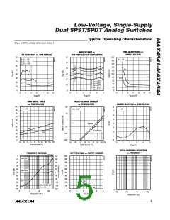
Test Circuits/Timing Diagrams
MAX4541
V+
t < 20ns
t < 20ns
f
r
MAX4542
+3V
0
LOGIC
INPUT
SWITCH
OUTPUT
MAX4543
MAX4544
50%
V+
COM
NO
or NC
V
OUT
SWITCH
INPUT
R
C
L
1k
L
t
OFF
35pF
IN
V
OUT
0.9 · V
0.9 · V
0UT
OUT
GND
0V
C INCLUDES FIXTURE AND STRAY CAPACITANCE.
LOGIC
INPUT
SWITCH
OUTPUT
0
t
ON
L
LOGIC INPUT WAVEFORMS INVERTED FOR SWITCHES
THAT HAVE THE OPPOSITE LOGIC SENSE.
R
L
V
OUT
= V
COM
(
)
R + R
L
ON
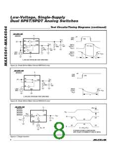
Figure 2. Switching Time
_______________________________________________________________________________________
7

 MAXIM [ MAXIM INTEGRATED PRODUCTS ]