±±15k EꢀDꢁ-rotected, ±µA, ±6Mbps, Dual/Quad
Lowꢁkoltage Level Translators in UCꢀ-
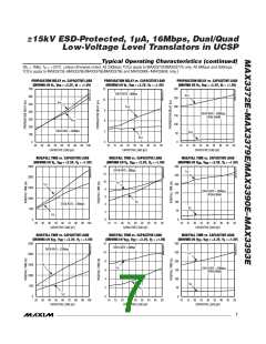
circuitry limits the maximum data rate for devices in the
MAX3372E–MAX3379E, MAX3390E–MAX3393E family to
16Mbps. The maximum data rate also depends heavily
on the load capacitance (see Typical Operating
Characteristics), output impedance of the driver, and the
operational voltage range (see Timing Characteristics).
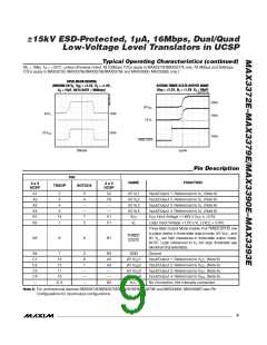
put mode. Connect THREE-STATE to V (logic high) for
L
normal operation. Activating the three-state output mode
disconnects the internal 10kΩ pullup resistors on the I/O
V
and I/O V lines. This forces the I/O lines to a high-
L
CC
impedance state, and decreases the supply current to
less than 1µA. The high-impedance I/O lines in three-
state output mode allow for use in a multidrop network.
When in three-state output mode, do not allow the voltage
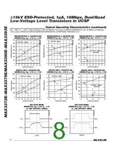
ꢀpeedꢁUp Circuitry
The MAX3373E–MAX3376E/MAX3378E/MAX3379E and
MAX3390E–MAX3393E feature a one-shot generator that
decreases the rise time of the output. When triggered,
MOSFETs PU1 and PU2 turn on for a short time to pull up
at I/O V to exceed (V + 0.3V), or the voltage at I/O
L_
L
V
CC_
to exceed (V + 0.3V).
CC
Thermal ꢀhortꢁCircuit -rotection
I/O V and I/O V
to their respective supplies (see
Thermal overload detection protects the MAX3372E–
MAX3379E and MAX3390E–MAX3393E from short-circuit
fault conditions. In the event of a short-circuit fault, when
L_
CC_
Figure 2b). This greatly reduces the rise time and propa-
gation delay for the low-to-high transition. The scope
photo of Rail-to-Rail Driving for 8Mbps Operation in the
Typical Operating Characteristics shows the speed-up
circuitry in operation.
the junction temperature (T ) reaches +152°C, a thermal
J
sensor signals the three-state output mode logic to force
the device into three-state output mode. When T has
J
cooled to +142°C, normal operation resumes.
Threeꢁꢀtate Output Mode
Pull THREE-STATE low to place the MAX3372E–
MAX3379E and MAX3390E–MAX3393E in three-state out-
V
V
L
CC
V
V
L
CC
V
V
CC
L
V
V
CC
L
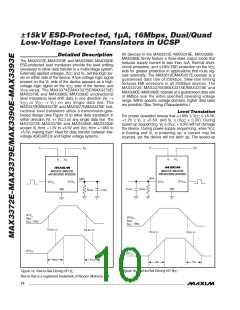
MAX3373E–MAX3376E,
MAX3378E/MAX3379E
MAX3372E–MAX3379E
AND MAX3390E–MAX3393E
AND MAX3390E–MAX3393E
DATA
DATA
I/O V
I/O V
CC_
L_
I/O V
I/O V
CC_
L_
C
LOAD
C
LOAD
GND
R
LOAD
GND
R
LOAD
I/O V
CC_
I/O V
L_
t
t
PD-VCC-HL
PD-VL-HL
t
t
PD-VL-LH
PD-VCC-LH
I/O V
I/O V
L_
CC_
t
t
t
RVL
t
FVL
RVCC
FVCC
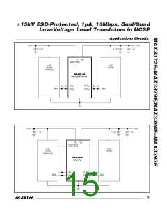
Figure 1c. Open-Drain Driving I/O V
Figure 1d. Open-Drain Driving I/O V
L
CC
______________________________________________________________________________________ 11

 MAXIM [ MAXIM INTEGRATED PRODUCTS ]