±±15k EꢀDꢁ-rotected, ±µA, ±6Mbps, Dual/Quad
Lowꢁkoltage Level Translators in UCꢀ-
All devices in the MAX3372E–MAX3379E, MAX3390E–
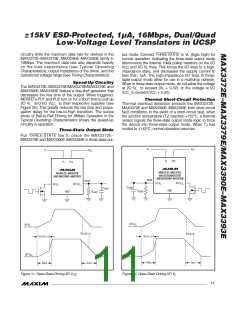
Detailed Description
MAX3393E family feature a three-state output mode that
The MAX3372E–MAX3379E and MAX3390E–MAX3393E
reduces supply current to less than 1µA, thermal short-
ESD-protected level translators provide the level shifting
circuit protection, and 15kV ESD protection on the V
CC
necessary to allow data transfer in a multivoltage system.
side for greater protection in applications that route sig-
nals externally. The MAX3372E/MAX3377E operate at a
guaranteed data rate of 230kbps. Slew-rate limiting
reduces EMI emissions in all 230kbps devices. The
MAX3373E–MAX3376E/MAX3378E/MAX3379E and
MAX3390E–MAX3393E operate at a guaranteed data rate
of 8Mbps over the entire specified operating voltage
range. Within specific voltage domains, higher data rates
are possible. (See Timing Characteristics.)
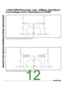
Externally applied voltages, V and V , set the logic lev-
CC
L
els on either side of the device. A low-voltage logic signal
present on the V side of the device appears as a high-
L
voltage logic signal on the V
side of the device, and
CC
vice-versa. The MAX3374E/MAX3375E/MAX3376E/
MAX3379E and MAX3390E–MAX3393E unidirectional
level translators level shift data in one direction (V
→
L
V
or V
→ V ) on any single data line. The
CC
CC L
MAX3372E/MAX3373E and MAX3377E/MAX3378E bidi-
rectional level translators utilize a transmission-gate-
based design (see Figure 2) to allow data translation in
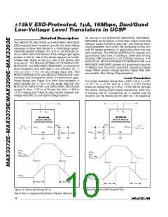
Level Translation
For proper operation ensure that +1.65V ≤ V
≤ +5.5V,
CC
either direction (V ↔ V ) on any single data line. The
L
CC
+1.2V ≤ V ≤ +5.5V, and V ≤ (V + 0.3V). During
L
L
CC
MAX3372E–MAX3379E and MAX3390E–MAX3393E
power-up sequencing, V ≥ (V + 0.3V) will not damage
L
CC
accept V from +1.2V to +5.5V and V from +1.65V to
L
CC
the device. During power-supply sequencing, when V
CC
+5.5V, making them ideal for data transfer between low-
is floating and V is powering up, a current may be
L
voltage ASICs/PLDs and higher voltage systems.
sourced, yet the device will not latch up. The speed-up
V
V
V
L
V
CC
L
CC
V
V
CC
V
V
CC
L
L
MAX3372E–MAX3379E
AND MAX3390E–MAX3393E
MAX3372E–MAX3379E
AND MAX3390E–MAX3393E
DATA
DATA
I/O V
_
I/O V
_
I/O V _
L
CC
I/O V _
L
CC
C
R
LOAD
GND
GND
LOAD
R
C
LOAD
LOAD
I/O V _
L
,
I/O V
_
CC
,
(t
RISE
FALL
(t
RISE
FALL
t
< 10ns)
t
< 10ns)
t
t
PD-VCC-LH
PD-VCC-HL
t
t
PD-VL-LH
PD-VL-HL
I/O V
_
CC
I/O V _
L
t
t
RVCC
FVCC
t
t
RVL
FVL
Figure 1b. Rail-to-Rail Driving I/O V
Figure 1a. Rail-to-Rail Driving I/O V
CC
L
Rail-to-Rail is a registered trademark of Nippon Motorola, Ltd.
10 ______________________________________________________________________________________

 MAXIM [ MAXIM INTEGRATED PRODUCTS ]