1.5µA I , Step-Up DC-DC Converters
Q
in Thin SOT23-5
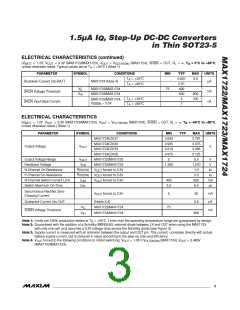
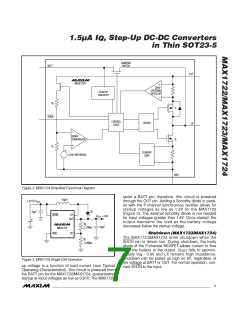
DAMPING
SWITCH
BATT
OUT
MAX1724
ZERO-
CROSSING
STARTUP
DETECTOR
CIRCUITRY
R
2
P
SHDN
CONTROL
LOGIC
DRIVER
LX
ERROR
COMPARATOR
N
R
1
CURRENT
LIMIT
1.235V REFERENCE
GND
Figure 2. MAX1724 Simplified Functional Diagram
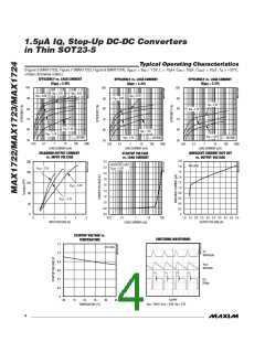
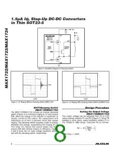
lacks a BATT pin; therefore, this circuit is powered
through the OUT pin. Adding a Schottky diode in paral-
lel with the P-channel synchronous rectifier allows for
startup voltages as low as 1.2V for the MAX1723
(Figure 3). The external Schottky diode is not needed
for input voltages greater than 1.8V. Once started, the
output maintains the load as the battery voltage
decreases below the startup voltage.
10µH
1.2V TO V
OUT
D1
10µF
LX
OUT
SHDN
V
= 3.6V
OUT
R2
10µF
2.37MΩ
MAX1723
GND
FB
Shutdown (MAX1723/MAX1724)
The MAX1723/MAX1724 enter shutdown when the
SHDN pin is driven low. During shutdown, the body
diode of the P-channel MOSFET allows current to flow
R1
1.24MΩ
from the battery to the output. V
falls to approxi-
OUT
mately V - 0.6V and LX remains high impedance.
IN
Shutdown can be pulled as high as 6V, regardless of
the voltage at BATT or OUT. For normal operation, con-
nect SHDN to the input.
Figure 3. MAX1723 Single-Cell Operation
up voltage is a function of load current (see Typical
Operating Characteristics). This circuit is powered from
the BATT pin for the MAX1722/MAX1724, guaranteeing
startup at input voltages as low as 0.91V. The MAX1723
_______________________________________________________________________________________
7

 MAXIM [ MAXIM INTEGRATED PRODUCTS ]