1.5µA I , Step-Up DC-DC Converters
Q
in Thin SOT23-5
Table 2. Suggested Surface-Mount Capacitors and Manufacturers (C1 and C2)
CAPACITOR
VALUE
PHONE
WEBSITE
MANUFACTURER
DESCRIPTION
1µF to 10µF
X7R Ceramic
843-448-9411
www.avxcorp.com
AVX
TAJ Tantalum Series
TPS Tantalum Series
10µF to 330µF
1µF to 22µF
10µF to 330µF
68µF to 330µF
X5R/X7R Ceramic
T494 Tantalum Series
T520 Tantalum Series
864-963-6300
www.kemet.com
Kemet
408-749-9714
www.secc.co.jp
Sanyo
33µF to 330µF
33µF to 330µF
1µF to 10µF
TPC Polymer Series
X5R/X7R Ceramic
X7R Ceramic
800-368-2496
www.t-yuden.org
Taiyo Yuden
TDK
847-803-6100
www.tdk.com
594D Tantalum Series
595D Tantalum Series
203-452-5664
www.vishay.com
Vishay Sprague
10µF to 330µF
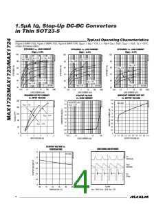
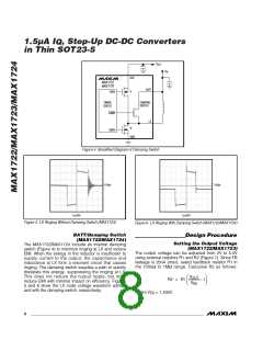
For most applications, the peak inductor current equals
the current limit. However, for applications using large
inductor values or low input voltages, the maximum on-
time limits the peak inductor current (see Inductor
Selection section).
where I
is the peak inductor current (see Inductor
PEAK
Selection section). For ceramic capacitors, the output
voltage ripple is typically dominated by V
. For
RIPPLE(C)
example, a 10µF ceramic capacitor and a 10µH induc-
tor typically provide 75mV of output ripple when step-
ping up from 3.3V to 5V at 50mA. Low input-to-output
voltage differences (i.e. two cells to 3.3V) require high-
er output capacitor values.
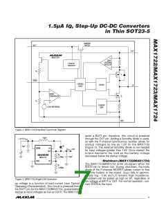
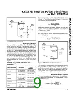
Capacitor Selection
Choose input and output capacitors to supply the input
and output peak currents with acceptable voltage rip-
Capacitance and ESR variation of temperature should
be considered for best performance in applications
with wide operating temperature ranges. Table 2 lists
suggested capacitors and suppliers.
ple. The input filter capacitor (C ) reduces peak cur-
IN
rents drawn from the battery and improves efficiency.
Low equivalent series resistance (ESR) capacitors are
recommended. Ceramic capacitors have the lowest
ESR, but low ESR tantalum or polymer capacitors offer
a good balance between cost and performance.
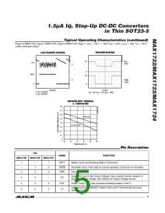
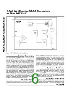
PC Board Layout Considerations
Output voltage ripple has two components: variations
in the charge stored in the output capacitor with each
LX pulse, and the voltage drop across the capacitor’s
ESR caused by the current into and out of the capaci-
tor:
Careful PC board layout is important for minimizing
ground bounce and noise. Keep the IC’s GND pin and
the ground leads of the input and output capacitors
less than 0.2in (5mm) apart using a ground plane. In
addition,
keep
all
connections
to
FB
(MAX1722/MAX1723 only) and LX as short as possible.
VRIPPLE = VRIPPLE C + VRIPPLE ESR
(
)
(
)
Chip Information
VRIPPLE ESR ≈ IPEAK RESR COUT
(
)
(
)
TRANSISTOR COUNT: 863
1
2
L
2
2
VRIPPLE C
≈
I
(
-IOUT
)
PEAK
(
)
V
OUT -VBATT C
(
)
OUT
10 ______________________________________________________________________________________

 MAXIM [ MAXIM INTEGRATED PRODUCTS ]