Complete, Isolated RS-485/RS-422
Data Interface
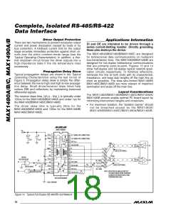
Driver Output Protection
___________Applications Information
There are two mechanisms to prevent excessive output
current and power dissipation caused by faults or by
bus contention. A foldback current limit on the output
stage provides immediate protection against short cir-
cuits over the entire common-mode range (see the
Typical Operating Characteristics). In addition, a ther-
mal shutdown circuit forces the driver outputs into a
high-impedance state if the die temperature rises
excessively.
DI and DE are intended to be driven through a
series current-limiting resistor. Directly grounding
these pins destroys the device.
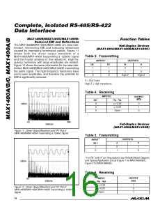
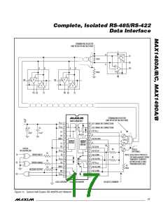
The MAX1480A/MAX1480B/MAX1480C are designed
for bidirectional data communications on multipoint
bus-transmission lines. The MAX1490A/MAX1490B are
designed for full-duplex bidirectional communications
that are primarily point-to-point. Figures 13 and 14
show half-duplex and full-duplex typical network appli-
cation circuits, respectively. To minimize reflections,
terminate the line at both ends with its characteristic
impedance, and keep stub lengths off the main line as
short as possible. The slew-rate-limited MAX1480B/
MAX1480C/MAX1490B are more tolerant of imperfect
termination and stubs off the main line.
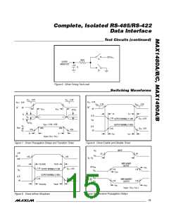
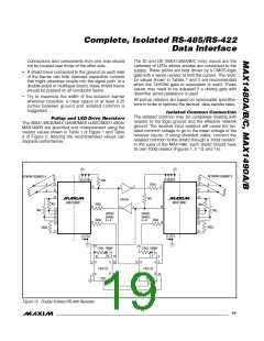
Propagation Delay Skew
Typical propagation delays are shown in the Typical
Operating Characteristics using the test circuit of
Figure 5. Propagation delay skew is simply the differ-
ence between the low-to-high and high-to-low propaga-
tion delay. Small driver/receiver skew times help
reduce EMI and reflections by maintaining balanced
differential signals.
Layout Considerations
The MAX1480A/MAX1480B/MAX1480C/MAX1490A/
MAX1490B pinouts enable optimal PC board layout by
minimizing interconnect lengths and crossovers.
The receiver skew time, t
100ns for the MAX1480A/MAX1490A and under 1µs for
the MAX1480B/MAX1480C/MAX1490B.
- t
, is typically under
PLH PHL
I
I
• For maximum isolation, the “isolation barrier” should
not be breached except by the MAX1480A/
MAX1480B/MAX1480C/MAX1490A/MAX1490B.
The driver skew time is typically 25ns for the
MAX1480A/MAX1490A and 100ns for the MAX1480B/
MAX1480C/MAX1490B.
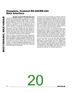
MAX1490A/B
V
IN
5V
V
V
CC1
AC1 (MAKE NO CONNECTION)
1
2
C1
C2
24
23
22
21
20
19
18
17
16
15
14
13
CC2
AC2 (MAKE NO CONNECTION)
22µF
0.1µF
ISO V
CC1
D1
D2
3
Y
120Ω
ISO RO DRV
4
D
R
DI
120Ω
GND1
Z
A
A
B
Z
Y
5
SHIELD (OPTIONAL)
B
FS
6
SD
Z
7
120Ω
74HC86
B
V
CC3
Y
8
OR EQUIVALENT
120Ω
RO
R1
R2
R5, 100Ω
DI
ISO COM1
DI
SH1
9
A
R4
SHIELD (OPTIONAL)
DI´
V
ISO DI DRV
SH2
CC4
10
11
12
DRIVER INPUT
ISO V
CC2
RO
R6, 100Ω
RO
NOTE: RESISTORS R5 AND R6 PROTECT
THE MAX1490A/B FROM TRANSIENT
CURRENTS BETWEEN SHIELD AND
TRANSMISSION LINES.
R3
RECEIVER OUTPUT
ISO RO LED
GND2
ISOLATED COMMON
ISOLATION BARRIER
LOGIC GROUND
Figure 14. Typical Full-Duplex RS-485/RS-422 Network
18 ______________________________________________________________________________________

 MAXIM [ MAXIM INTEGRATED PRODUCTS ]