MAX11120–MAX11128
1Msps, Low-Power, Serial 12-/10-/8-Bit,
4-/8-/16-Channel ADCs
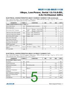
ELECTRICAL CHARACTERISTICS (MAX11122/MAX11125/MAX11128) (continued)
(V
= 2.35V to 3.6V, V
= 1.5V to 3.6V, f
= 1Msps, f
= 16MHz, 50% duty cycle, V
= V , T = -40NC to +125NC,
DD
OVDD
SAMPLE
SCLK
REF+ DD A
unless otherwise noted. Typical values are at T = +25NC.) (Note 2)
A
PARAMETER
SYMBOL
CONDITIONS
MIN
TYP
MAX
UNITS
TIMING CHARACTERISTICS (Figure 1) (Note 11)
SCLK Clock Period
SCLK Duty Cycle
t
Externally clocked conversion
62.4
40
4
ns
%
CP
t
60
16.5
15
CH
V
V
= 1.5V to 2.35V
= 2.35V to 3.6V
C
10pF
=
OVDD
LOAD
SCLK Fall to DOUT Transition
t
ns
DOT
4
OVDD
16th SCLK Fall to DOUT Disable
14th SCLK Fall to DOUT Disable
SCLK Fall to DOUT Enable
DIN to SCLK Rise Setup
SCLK Rise to DIN Hold
t
C
C
C
= 10pF, channel ID on
= 10pF, channel ID off
= 10pF
15
ns
ns
ns
ns
ns
ns
ns
ns
DOD
LOAD
LOAD
LOAD
16
t
14
DOE
t
4
1
4
1
5
DS
DH
t
t
CS Fall to SCLK Fall Setup
SCLK Fall to CS Fall Hold
CNVST Pulse Width
CSS
CSH
t
t
See Figure 6
CSW
CS or CNVST Rise to EOC Low
(Note 7)
t
See Figure 7, f
= 1Msps
5.3
6.2
Fs
CNV_INT
SAMPLE
t
5
ns
CS Pulse Width
CSBW
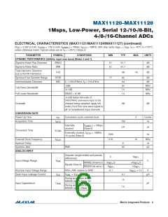
ELECTRICAL CHARACTERISTICS (MAX11121/MAX11124/MAX11127)
(V
= 2.35V to 3.6V, V
= 1.5V to 3.6V, f
= 1Msps, f
= 16MHz, 50% duty cycle, V
= V , T = -40NC to +125NC,
DD
OVDD
SAMPLE
SCLK
REF+ DD A
unless otherwise noted. Typical values are at T = +25NC.) (Note 2)
A
PARAMETER
DC ACCURACY (Notes 3 and 4)
Resolution
SYMBOL
CONDITIONS
MIN
TYP
MAX
UNITS
RES
INL
10 bit
10
Bits
LSB
LSB
LSB
LSB
Integral Nonlinearity
Differential Nonlinearity
Offset Error
0.4
0.4
1.0
1.0
DNL
No missing codes
(Note 5)
0.5
Gain Error
-0.2
Offset Error Temperature
Coefficient
OE
GE
2
ppm/NC
ppm/NC
LSB
TC
Gain Temperature Coefficient
0.8
0.5
0.1
TC
Channel-to-Channel Offset
Matching
Line Rejection
PSR
(Note 6)
0.3
LSB/V
����������������������������������������������������������������� Maxim Integrated Products
5

 MAXIM [ MAXIM INTEGRATED PRODUCTS ]