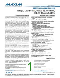
MAX11120–MAX11128
1Msps, Low-Power, Serial 12-/10-/8-Bit,
4-/8-/16-Channel ADCs
ABSOLUTE MAXIMUM RATINGS
DD
V
to GND.............................................................-0.3V to +4V
Continuous Power Dissipation (T = +70NC)
A
OVDD, AIN0–AIN13, CNVST/AIN14, REF+, REF-/AIN15
TQFN (derate 34.4mW/NC above +70NC)..................2758mW
Operating Temperature Range........................ -40NC to +125NC
Junction Temperature .....................................................+150NC
Storage Temperature Range............................ -65NC to +150NC
Lead Temperature (soldering, 10s) ................................+300NC
Soldering Temperature (reflow) ......................................+260NC
to GND......................-0.3V to the lower of (V + 0.3V) and +4V
DD
CS, SCLK, DIN, DOUT, EOC TO GND ..... -0.3V to the Lower of
(V + 0.3V) and +4V
OVDD
DGND to GND......................................................-0.3V to +0.3V
Input/Output Current (all pins) ...........................................50mA
Stresses beyond those listed under “Absolute Maximum Ratings” may cause permanent damage to the device. These are stress ratings only, and functional opera-
tion of the device at these or any other conditions beyond those indicated in the operational sections of the specifications is not implied. Exposure to absolute
maximum rating conditions for extended periods may affect device reliability.
PACKAGE THERMAL CHARACTERISTICS (Note 1)
TQFN
Junction-to-Ambient Thermal Resistance (B )...........29NC/W
JA
Junction-to-Case Thermal Resistance (B )..................2NC/W
JC
Note 1: Package thermal resistances were obtained using the method described in JEDEC specification JESD51-7, using a four-
layer board. For detailed information on package thermal considerations, refer to www.maxim-ic.com/thermal-tutorial.
ELECTRICAL CHARACTERISTICS (MAX11122/MAX11125/MAX11128)
(V
= 2.35V to 3.6V, V
= 1.5V to 3.6V, f
= 1Msps, f
= 16MHz, 50% duty cycle, V
= V , T = -40NC to +125NC,
DD
OVDD
SAMPLE
SCLK
REF+ DD A
unless otherwise noted. Typical values are at T = +25NC.) (Note 2)
A
PARAMETER
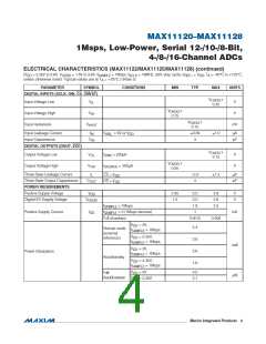
DC ACCURACY (Notes 3 and 4)
Resolution
SYMBOL
CONDITIONS
MIN
TYP
MAX
UNITS
RES
INL
12 bit
12
Bits
LSB
LSB
LSB
LSB
Integral Nonlinearity
Differential Nonlinearity
Offset Error
1.0
1.0
2.5
4.0
DNL
No missing codes
(Note 5)
0.7
Gain Error
-0.5
Offset Error Temperature
Coefficient
OE
GE
2
ppm/NC
ppm/NC
LSB
TC
Gain Temperature Coefficient
0.8
0.5
0.4
TC
Channel-to-Channel Offset
Matching
Line Rejection
PSR
(Note 6)
1.5
-78
LSB/V
DYNAMIC PERFORMANCE (250kHz, input sine wave) (Notes 3 and 7)
Signal-to-Noise Plus Distortion
Signal-to-Noise Ratio
SINAD
SNR
70
70
72.5
72.6
dB
dB
Total Harmonic Distortion
(Up to the 5th Harmonic)
THD
-87
dB
Spurious-Free Dynamic Range
Intermodulation Distortion
SFDR
IMD
79
88
dB
dB
f = 249.878kHz, f = 219.97kHz
-85
1
2
����������������������������������������������������������������� Maxim Integrated Products
2

 MAXIM [ MAXIM INTEGRATED PRODUCTS ]