MAX11120–MAX11128
1Msps, Low-Power, Serial 12-/10-/8-Bit,
4-/8-/16-Channel ADCs
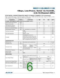
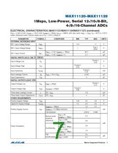
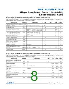
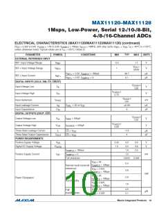
ELECTRICAL CHARACTERISTICS (MAX11120/MAX11123/MAX11126) (continued)
(V
= 2.35V to 3.6V, V
= 1.5V to 3.6V, f
= 1Msps, f
= 16MHz, 50% duty cycle, V
= V , T = -40NC to +125NC,
DD
OVDD
SAMPLE
SCLK
REF+
DD
A
unless otherwise noted. Typical values are at T = +25NC.) (Note 2)
A
PARAMETER
SYMBOL
CONDITIONS
MIN
TYP
MAX
UNITS
DYNAMIC PERFORMANCE (250kHz, input sine wave) (Notes 3 and 7)
Signal-to-Noise Plus Distortion
Signal-to-Noise Ratio
SINAD
SNR
49
49
49.6
49.6
dB
dB
Total Harmonic Distortion
(Up to the 5th Harmonic)
THD
-77
-66
dB
Spurious-Free Dynamic Range
Intermodulation Distortion
SFDR
IMD
63
69
-75
50
dB
dB
f = 249.878kHz, f = 219.97kHz
1
2
-3dB
MHz
MHz
MHz
Full-Power Bandwidth
Full-Linear Bandwidth
-0.1dB
7.5
1.5
SINAD > 49dB
-0.5dB below full-scale of 249.878kHz sine-
wave input to the channel being sampled;
apply full-scale 219.97kHz sine wave signal
to all 15 nonselected input channels
Crosstalk
-88
dB
CONVERSION RATE
Power-Up Time
t
Conversion cycle, external clock
2
Cycles
ns
PU
Acquisition Time
t
156
5.9
ACQ
f
= 1Msps
SAMPLE
(Note 8)
Internally clocked
µs
ns
Conversion Time
t
CONV
Externally clocked, f
cycles (Note 8)
= 16MHz, 16
SCLK
1000
0.16
External Clock Frequency
Aperture Delay
f
16
MHz
ns
SCLK
8
Aperture Jitter
RMS
30
ps
ANALOG INPUT
Unipolar (single-ended and pseudo
differential)
0
V
REF+
Input Voltage Range
V
V
INA
RANGE bit set to 0
RANGE bit set to 1
-V
/2
+V
/2
REF+
REF+
Bipolar (Note 9)
-V
+V
REF+
REF+
V
+
REF+
0.1
Absolute Input Voltage Range
Static Input Leakage Current
AIN+, AIN- relative to GND
= V , GND
-0.1
V
I
V
-0.1
FA
ILA
AIN_
DD
During acquisition time,
RANGE bit = 0 (Note 10)
15
Input Capacitance
C
pF
AIN
During acquisition time,
RANGE bit = 1 (Note 10)
7.5
����������������������������������������������������������������� Maxim Integrated Products
9

 MAXIM [ MAXIM INTEGRATED PRODUCTS ]