MAX11120–MAX11128
1Msps, Low-Power, Serial 12-/10-/8-Bit,
4-/8-/16-Channel ADCs
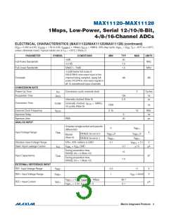
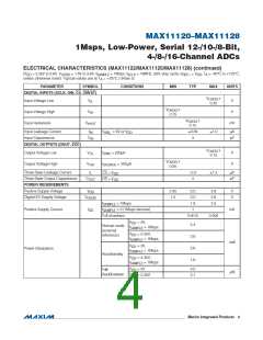
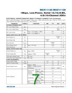
ELECTRICAL CHARACTERISTICS (MAX11122/MAX11125/MAX11128) (continued)
(V
= 2.35V to 3.6V, V
= 1.5V to 3.6V, f
= 1Msps, f
= 16MHz, 50% duty cycle, V
= V , T = -40NC to +125NC,
DD
OVDD
SAMPLE
SCLK
REF+ DD A
unless otherwise noted. Typical values are at T = +25NC.) (Note 2)
A
PARAMETER
SYMBOL
CONDITIONS
MIN
TYP
MAX
UNITS
DIGITAL INPUTS (SCLK, DIN, CS, CNVST)
V
O
OVDD
0.25
Input Voltage Low
Input Voltage High
Input Hysteresis
V
V
V
IL
V
O
OVDD
0.75
V
IH
V
O
OVDD
0.15
V
mV
HYST
Input Leakage Current
I
V
= 0V or V
DD
0.09
3
1.0
FA
IN
AIN_
Input Capacitance
C
pF
IN
DIGITAL OUTPUTS (DOUT, EOC)
V
O
OVDD
0.15
Output Voltage Low
Output Voltage High
V
I
I
= 200FA
V
V
OL
SINK
V
O
OVDD
0.85
V
= 200FA
OH
SOURCE
Three-State Leakage Current
Three-State Output Capacitance
POWER REQUIREMENTS
Positive Supply Voltage
I
-0.3
1.5
FA
CS = V
CS = V
L
DD
C
4
pF
OUT
DD
V
2.35
1.5
3.0
3.0
1.8
1
3.6
3.6
2.5
V
V
DD
Digital I/O Supply Voltage
V
OVDD
f
f
= 1Msps
SAMPLE
Positive Supply Current
I
= 0 (1Msps devices)
mA
DD
SAMPLE
Full shutdown
0.0015
0.006
V
= 3V,
DD
5.4
Normal mode
(external
reference)
f
= 1Msps
SAMPLE
V
= 2.35V,
DD
3.8
2.6
1.6
f
= 1Msps
SAMPLE
mW
V
= 3V,
DD
Power Dissipation
f
= 1Msps
SAMPLE
AutoStandby
V
= 2.35V,
DD
f
= 1Msps
SAMPLE
V
V
= 3V
4.5
2.1
Full/
AutoShutdown
DD
FW
= 2.35V
DD
����������������������������������������������������������������� Maxim Integrated Products
4

 MAXIM [ MAXIM INTEGRATED PRODUCTS ]