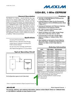
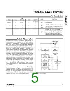
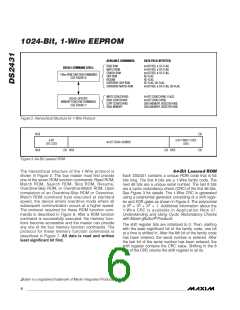
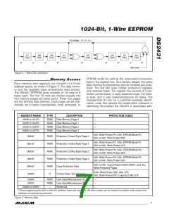
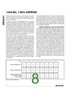
1024-Bit, 1-Wire EEPROM
DS2431
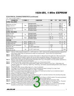
ELECꢂRICꢁL CHꢁRꢁCꢂERISꢂICS (continued)
(T = -40°C to +85°C.) (Note 1)
A
PARAMETER
SYMBOL
CONDITIONS
MIN
TYP
MAX
UNITS
IO PIN: 1-Wire WRITE
Standard speed
60
5
120
15.5
15.5
15
Write-Zero Low Time
(Notes 2, 16, 17)
t
µs
µs
Overdrive speed, V
Overdrive speed
Standard speed
Overdrive speed
> 4.5V
W0L
PUP
6
1
Write-One Low Time
(Notes 2, 17)
t
W1L
1
2
IO PIN: 1-Wire READ
Standard speed
Overdrive speed
Standard speed
Overdrive speed
5
1
15 - ꢁ
2 - ꢁ
15
Read Low Time
(Notes 2, 18)
t
µs
µs
RL
t
t
+ ꢁ
Read Sample Time
(Notes 2, 18)
RL
RL
t
MSR
+ ꢁ
2
EEPROM
Programming Current
Programming Time
I
t
(Notes 5, 19)
(Notes 20, 21)
At +25°C
0.8
10
mA
ms
PROG
PROG
200k
50k
Write/Erase Cycles (Endurance)
(Notes 22, 23)
N
CY
ꢂ
At +85°C (worst case)
Data Retention
(Notes 24, 25, 26)
t
At +85°C (worst case)
40
Years
DR
Note 1: Limits are 100% production tested at T = +25°C and/or T = +85°C. Limits over the operating temperature range and rel-
A
A
evant supply voltage range are guaranteed by design and characterization. Typical values are not guaranteed.
Note 2: System requirement.
Note 3: Maximum allowable pullup resistance is a function of the number of 1-Wire devices in the system and 1-Wire recovery times.
The specified value here applies to systems with only one device and with the minimum 1-Wire recovery times. For more
heavily loaded systems, an active pullup such as that found in the DS2482-x00, DS2480B, or DS2490 may be required.
Note 4: Maximum value represents the internal parasite capacitance when V
is first applied. Once the parasite capacitance is
PUP
charged, it does not affect normal communication.
Note 5: Guaranteed by design, characterization, and/or simulation only. Not production tested.
Note 6: , V , and V are a function of the internal supply voltage, which is a function of V
V
, R , 1-Wire timing, and
PUP PUP
TL TH
HY
capacitive loading on IO. Lower V
, higher R
, shorter t
, and heavier capacitive loading all lead to lower values of
REC
PUP
PUP
V , V , and V
TL TH
.
HY
Note 7: Voltage below which, during a falling edge on IO, a logic 0 is detected.
Note 8: The voltage on IO must be less than or equal to V at all times the master is driving IO to a logic 0 level.
ILMAX
Note 9: Voltage above which, during a rising edge on IO, a logic 1 is detected.
Note 10: After V is crossed during a rising edge on IO, the voltage on IO must drop by at least V to be detected as logic 0.
TH
HY
Note 11: The I-V characteristic is linear for voltages less than 1V.
Note 12: Applies to a single device attached to a 1-Wire line.
Note 13: The earliest recognition of a negative edge is possible at t
after V has been reached on the preceding rising edge.
TH
REH
Note 14: Defines maximum possible bit rate. Equal to t
+ t
.
W0LMIN
RECMIN
Note 15: Interval after t
during which a bus master can read a logic 0 on IO if there is a DS2431 present. The power-up presence-
RSTL
detect pulse could be outside this interval, but will be complete within 2ms after power-up.
Note 16: Numbers in bold are not in compliance with legacy 1-Wire product standards. See the Comparison Table.
Note 17: ε in Figure 11 represents the time required for the pullup circuitry to pull the voltage on IO up from V to V . The actual
IL
TH
maximum duration for the master to pull the line low is t
+ t - ε and t
+ t - ε, respectively.
W0LMAX F
W1LMAX
F
Note 18: δ in Figure 11 represents the time required for the pullup circuitry to pull the voltage on IO up from V to the input-high
IL
threshold of the bus master. The actual maximum duration for the master to pull the line low is t
+ t .
RLMAX
F
_______________________________________________________________________________________
3

 MAXIM [ MAXIM INTEGRATED PRODUCTS ]