1024-Bit, 1-Wire EEPROM
Contact the factory to set up and register a custom
manufacturer ID. The last row is reserved for future
use. It is undefined in terms of R/W functionality and
should not be used.
The copy-protection byte is used for a higher level of
security and should only be used after all other protec-
tion control bytes, user bytes, and write-protected
pages are set to their final value. If the copy-protection
byte is set to 55h or AAh, all copy attempts to the regis-
ter row and user-byte row are blocked. In addition, all
copy attempts to write-protected main memory pages
(i.e., refresh) are blocked.
In addition to the main EEPROM array, an 8-byte
volatile scratchpad is included. Writes to the EEPROM
array are a two-step process. First, data is written to the
scratchpad and then copied into the main array. This
allows the user to first verify the data written to the
scratchpad prior to copying into the main array. The
device only supports full row (8-byte) copy operations.
For data in the scratchpad to be valid for a copy opera-
tion, the address supplied with a Write Scratchpad
command must start on a row boundary, and 8 full
bytes must be written into the scratchpad.
DS2431
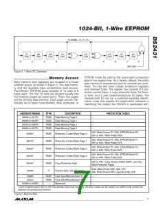
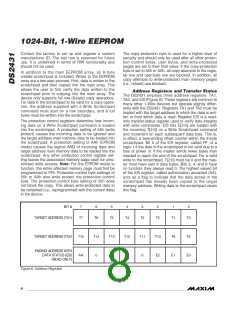
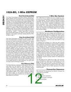
Address Registers and Transfer Status
The DS2431 employs three address registers: TA1,
TA2, and E/S (Figure 6). These registers are common to
many other 1-Wire devices but operate slightly differ-
ently with the DS2431. Registers TA1 and TA2 must be
loaded with the target address to which the data is writ-
ten or from which data is read. Register E/S is a read-
only transfer-status register used to verify data integrity
with write commands. E/S bits E[2:0] are loaded with
the incoming T[2:0] on a Write Scratchpad command
and increment on each subsequent data byte. This is,
in effect, a byte-ending offset counter within the 8-byte
scratchpad. Bit 5 of the E/S register, called PF, is a
logic 1 if the data in the scratchpad is not valid due to a
loss of power or if the master sends fewer bytes than
needed to reach the end of the scratchpad. For a valid
write to the scratchpad, T[2:0] must be 0 and the mas-
ter must have sent 8 data bytes. Bits 3, 4, and 6 have
no function; they always read 0. The highest valued bit
of the E/S register, called authorization accepted (AA),
acts as a flag to indicate that the data stored in the
scratchpad has already been copied to the target
memory address. Writing data to the scratchpad clears
this flag.
The protection control registers determine how incom-
ing data on a Write Scratchpad command is loaded
into the scratchpad. A protection setting of 55h (write
protect) causes the incoming data to be ignored and
the target address main memory data to be loaded into
the scratchpad. A protection setting of AAh (EPROM
mode) causes the logical AND of incoming data and
target address main memory data to be loaded into the
scratchpad. Any other protection control register set-
ting leaves the associated memory page open for unre-
stricted write access. Note: For the EPROM mode to
function, the entire affected memory page must first be
programmed to FFh. Protection-control byte settings of
55h or AAh also write protect the protection-control
byte. The protection-control byte setting of 55h does
not block the copy. This allows write-protected data to
be refreshed (i.e., reprogrammed with the current data)
in the device.
BIT #
7
6
5
4
3
2
1
0
TARGET ADDRESS (TA1)
T7
T6
T5
T4
T3
T2
T1
T0
TARGET ADDRESS (TA2)
T15
AA
T14
0
T13
PF
T12
0
T11
0
T10
E2
T9
E1
T8
E0
ENDING ADDRESS WITH
DATA STATUS (E/S)
(READ ONLY)
Figure 6. Address Registers
8
_______________________________________________________________________________________

 MAXIM [ MAXIM INTEGRATED PRODUCTS ]