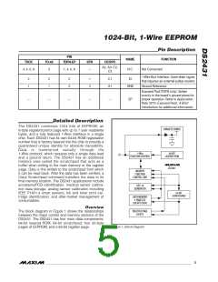
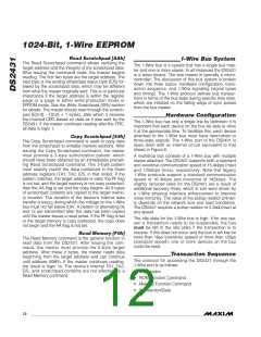
1024-Bit, 1-Wire EEPROM
DS2431
at standard speed (default, OD = 0) or at overdrive
speed (OD = 1). If not explicitly set into overdrive
mode, the DS2431 assumes standard speed.
Writing with Verification
To write data to the DS2431, the scratchpad must be
used as intermediate storage. First, the master issues
the Write Scratchpad command to specify the desired
target address, followed by the data to be written to the
scratchpad. Note that Copy Scratchpad commands
must be performed on 8-byte boundaries, i.e., the three
LSBs of the target address (T2, T1, T0) must be equal
to 000b. If T[2:0] are sent with nonzero values, the copy
function is blocked. Under certain conditions (see the
Write Scratchpad [0Fh] section) the master receives an
inverted CRC-16 of the command, address (actual
address sent), and data at the end of the Write
Scratchpad command sequence. Knowing this CRC
value, the master can compare it to the value it has cal-
culated to decide if the communication was successful
and proceed to the Copy Scratchpad command. If the
master could not receive the CRC-16, it should send
the Read Scratchpad command to verify data integrity.
As a preamble to the scratchpad data, the DS2431
repeats the target address TA1 and TA2 and sends the
contents of the E/S register. If the PF flag is set, data
did not arrive correctly in the scratchpad, or there was
a loss of power since data was last written to the
scratchpad. The master does not need to continue
reading; it can start a new trial to write data to the
scratchpad. Similarly, a set AA flag together with a
cleared PF flag indicates that the device did not recog-
nize the Write command.
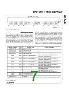
Write Scratchpad [0Fh]
The Write Scratchpad command applies to the data
memory and the writable addresses in the register
page. For the scratchpad data to be valid for copying
to the array, the user must perform a Write Scratchpad
command of 8 bytes starting at a valid row boundary.
The Write Scratchpad command accepts invalid
addresses and partial rows, but subsequent Copy
Scratchpad commands are blocked.
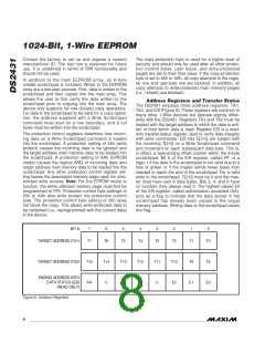
After issuing the Write Scratchpad command, the mas-
ter must first provide the 2-byte target address, fol-
lowed by the data to be written to the scratchpad. The
data is written to the scratchpad starting at the byte off-
set of T[2:0]. The E/S bits E[2:0] are loaded with the
starting byte offset and increment with each subse-
quent byte. Effectively, E[2:0] is the byte offset of the
last full byte written to the scratchpad. Only full data
bytes are accepted.
When executing the Write Scratchpad command, the
CRC generator inside the DS2431 (Figure 13) calcu-
lates a CRC of the entire data stream, starting at the
command code and ending at the last data byte as
sent by the master. This CRC is generated using the
CRC-16 polynomial by first clearing the CRC generator
and then shifting in the command code (0Fh) of the
Write Scratchpad command, the target addresses (TA1
and TA2), and all the data bytes. Note that the CRC-16
calculation is performed with the actual TA1 and TA2
and data sent by the master. The master can end the
Write Scratchpad command at any time. However, if
the end of the scratchpad is reached (E[2:0] = 111b),
the master can send 16 read time slots and receive the
CRC generated by the DS2431.
If everything went correctly, both flags are cleared.
Now the master can continue reading and verifying
every data byte. After the master has verified the data,
it can send the Copy Scratchpad command, for exam-
ple. This command must be followed exactly by the
data of the three address registers, TA1, TA2, and E/S.
The master should obtain the contents of these regis-
ters by reading the scratchpad.
If a Write Scratchpad command is attempted to a write-
protected location, the scratchpad is loaded with the
data already existing in memory rather than the data
transmitted. Similarly, if the target address page is in
EPROM mode, the scratchpad is loaded with the bit-
wise logical AND of the transmitted data and data
already existing in memory.
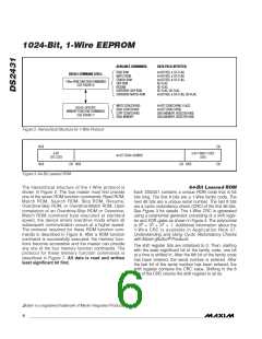
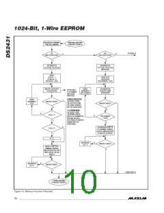
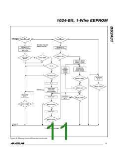
Memory Function Commands
The Memory Function Flowchart (Figure 7) describes
the protocols necessary for accessing the memory of
the DS2431. An example on how to use these functions
to write to and read from the device is in the Memory
Function Example section. The communication
between the master and the DS2431 takes place either
_______________________________________________________________________________________
9

 MAXIM [ MAXIM INTEGRATED PRODUCTS ]