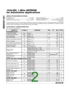
1024-Bit, 1-Wire EEPROM
for Automotive Applications
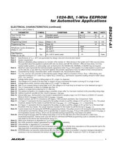
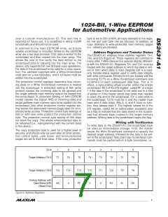
Comparisons Table
LEGACY VALUES
DS2431-A1 VALUES
PARAMETER
STANDARD SPEED (μs) OVERDRIVE SPEED (μs) STANDARD SPEED (μs) OVERDRIVE SPEED (μs)
MIN
MAX
MIN
MAX
MIN
MAX
MIN
MAX
t
SLOT
*
*
61
(undefined)
7
(undefined)
65
(undefined)
8
(undefined)
(including t
)
REC
t
480
15
(undefined)
48
2
80
6
480
15
640
60
48
2
80
6
RSTL
t
60
PDH
DS243-A1
t
60
240
120
8
24
16
60
240
120
8
24
PDL
t
60
6
60
6
15.5
W0L
*Intentional change, longer recovery time requirement due to modified 1-Wire front-end.
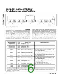
Pin Description
PIN
1
NAME
GND
I/O
FUNCTION
Ground Reference
2
1-Wire Bus Interface. Open drain, requires external pullup resistor.
No Connection
3–6
N.C.
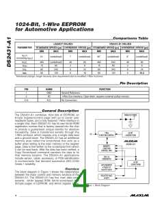
General Description
The DS2431-A1 combines 1024 bits of EEPROM, an
8-byte register/control page with up to seven user
read/write bytes, and a fully featured 1-Wire interface in
a single chip. Each DS2431-A1 has its own 64-bit ROM
registration number that is factory lasered into the chip
to provide a guaranteed unique identity for absolute
traceability. Data is transferred serially through the
1-Wire protocol, which requires only a single data lead
and a ground return. The DS2431-A1 has an additional
memory area called the scratchpad that acts as a
buffer when writing to the main memory or the register
page. Data is first written to the scratchpad from which
it can be read back. After the data has been verified, a
Copy Scratchpad command transfers the data to its
final memory location. The DS2431-A1 applications
include sensor, cable, accessory, or PCB identification
in environments that demand automotive AEC-Q100
Grade 1 reliability.
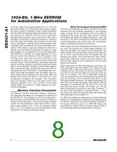
PARASITE POWER
1-Wire
FUNCTION CONTROL
64-BIT
LASERED ROM
I/O
DS2431-A1
MEMORY
FUNCTION
CONTROL UNIT
CRC-16
GENERATOR
64-BIT
SCRATCHPAD
DATA MEMORY
4 PAGES OF
Overview
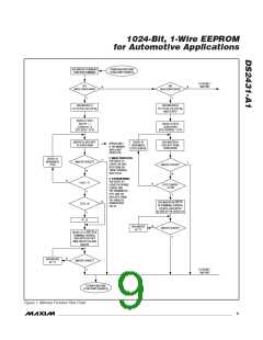
The block diagram in Figure 1 shows the relationships
between the major control and memory sections of the
DS2431-A1. The DS2431-A1 has four main data com-
ponents: 64-bit lasered ROM, 64-bit scratchpad, four
32-byte pages of EEPROM, and 64-bit register page.
256 BITS EACH
REGISTER PAGE
64 BITS
Figure 1. Block Diagram
4
_______________________________________________________________________________________

 MAXIM [ MAXIM INTEGRATED PRODUCTS ]