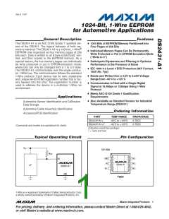
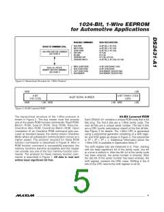
1024-Bit, 1-Wire EEPROM
for Automotive Applications
DS243-A1
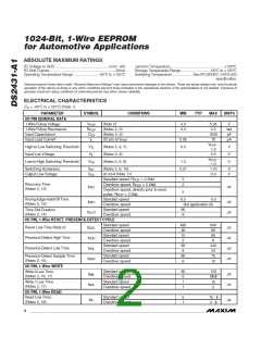
ELECTRICAL CHARACTERISTICS (continued)
(T = -40°C to +125°C) (Note 1)
A
PARAMETER
SYMBOL
CONDITIONS
Standard speed
MIN
TYP
MAX
15
UNITS
t
t
+ ꢁ
Read Sample Time
(Notes 2, 18)
RL
t
μs
MSR
Overdrive speed
+ ꢁ
2
RL
EEPROM
Programming Current
Programming Time
I
t
(Notes 5, 19)
(Note 20)
0.8
10
mA
ms
PROG
PROG
At +25°C
At +85°C
At +125°C
200k
50k
1k
Write/Erase Cycles (Endurance)
(Notes 21, 22)
N
CY
ꢂ
Data Retention
(Notes 23, 24, 25)
t
At +125°C (worst case)
10
Years
DR
Note 1: Specifications at T = -40°C are guaranteed by design only and not production tested.
A
Note 2: System requirement.
Note 3: Maximum allowable pullup resistance is a function of the number of 1-Wire devices in the system and 1-Wire recovery times.
The specified value here applies to systems with only one device and with the minimum 1-Wire recovery times. For more
heavily loaded systems, an active pullup such as that found in the DS2482-x00, DS2480B, or DS2490 may be required.
Note 4: Maximum value represents the internal parasite capacitance when V
is first applied. If a 2.2kΩ resistor is used to pull
PUP
up the data line, 2.5µs after V
has been applied, the parasite capacitance does not affect normal communications.
PUP
Note 5: Guaranteed by design, characterization, and/or simulation only. Not production tested.
Note 6: , V , and V are a function of the internal supply voltage, which is a function of V
V
, R , 1-Wire timing, and
PUP PUP
TL TH
HY
capacitive loading on I/O. Lower V , higher R , shorter t
PUP PUP
, and heavier capacitive loading all lead to lower values
REC
of V , V , and V
.
TL TH
HY
Note 7: Voltage below which, during a falling edge on I/O, a logic 0 is detected.
Note 8: The voltage on I/O needs to be less than or equal to V at all times the master is driving I/O to a logic-0 level.
ILMAX
Note 9: Voltage above which, during a rising edge on I/O, a logic 1 is detected.
Note 10: After V is crossed during a rising edge on I/O, the voltage on I/O must drop by at least V to be detected as logic 0.
TH
HY
Note 11: The I-V characteristic is linear for voltages less than 1V.
Note 12: Applies to a single device attached to a 1-Wire line.
Note 13: The earliest recognition of a negative edge is possible at t
after V has been reached on the preceding rising edge.
TH
REH
Note 14: Defines maximum possible bit rate. Equal to t
+ t
.
W0LMIN
RECMIN
Note 15: Interval after t
during which a bus master is guaranteed to sample a logic 0 on I/O if there is a DS2431-A1 present.
RSTL
Minimum limit is t
; maximum limit is t
+ t
.
PDHMAX
PDHMIN
PDLMIN
Note 16: Bolded numbers are NOT in compliance with legacy 1-Wire product standards. See Comparisons Table.
Note 17: ε in Figure 11 represents the time required for the pullup circuitry to pull the voltage on I/O up from V to V . The actual
IL
TH
maximum duration for the master to pull the line low is t
+ t - ε and t
+ t - ε, respectively.
W0LMAX F
W1LMAX
F
Note 18: δ in Figure 11 represents the time required for the pullup circuitry to pull the voltage on I/O up from V to the input-high
IL
threshold of the bus master. The actual maximum duration for the master to pull the line low is t
+ t .
RLMAX
F
Note 19: Current drawn from I/O during the EEPROM programming interval. The pullup circuit on I/O during the programming inter-
val should be such that the voltage at I/O is greater than or equal to V . If V in the system is close to V , a
PUPMIN
PUP
PUPMIN
low-impedance bypass of R
, which can be activated during programming, may need to be added.
PUP
Note 20: Interval begins t
after the trailing rising edge on I/O for the last time slot of the E/S byte for a valid Copy
REHMAX
Scratchpad sequence. Interval ends once the device’s self-timed EEPROM programming cycle is complete and the cur-
rent drawn by the device has returned from I to I .
PROG
L
Note 21: Write-cycle endurance is degraded as T increases.
A
Note 22: Not 100% production tested; guaranteed by reliability monitor sampling.
Note 23: Data retention is degraded as T increases.
A
Note 24: Guaranteed by 100% production test at elevated temperature for a shorter time; equivalence of this production test to the
data sheet limit at operating temperature range is established by reliability testing.
Note 25: EEPROM writes can become nonfunctional after the data-retention time is exceeded. Long-term storage at elevated tem-
peratures is not recommended; the device can lose its write capability after 10 years at +125°C or 40 years at +85°C.
_______________________________________________________________________________________
3

 MAXIM [ MAXIM INTEGRATED PRODUCTS ]