Signal Description
Pin Description
The RGMII interface supports 10/100/1000BASE-T and 1000BASE-X modes of operation.The RGMII interface
pins are also used for the RTBI interface. See Table 5 for RTBI pin definitions. The MAC interface pins are 3.3V
tolerant.
Table 4:
RGMII Interface
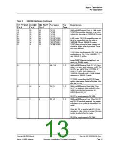
117-TFBGA 96-BCC 128-PQFP Pin Name
Pin
Description
Pin #
Pin #
Pin #
Type
E2
8
14
GTX_CLK/
TXC
I
RGMII Transmit Clock provides a 125 MHz,
25 MHz, or 2.5 MHz reference clock with ±
50 ppm tolerance depending on speed. In
RGMII mode, GTX_CLK is used as TXC.
H2
G3
G2
F1
16
14
12
11
24
20
19
18
TXD[3]/TD[3]
TXD[2]/TD[2]
TXD[1]/TD[1]
TXD[0]/TD[0]
I
RGMII Transmit Data. In RGMII mode,
TXD[3:0] are used as TD[3:0].
In RGMII mode, TXD[3:0] run at double data
rate with bits [3:0] presented on the rising
edge of GTX_CLK, and bits [7:4] presented
on the falling edge of GTX_CLK. In this
mode, TXD[7:4] are ignored.
In RGMII 10/100BASE-T modes, the trans-
mit data nibble is presented on TXD[3:0] on
the rising edge of GTX_CLK.
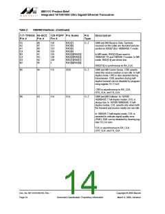
E1
9
16
TX_EN/
TX_CTL
I
RGMII Transmit Control. In RGMII mode,
TX_EN is used as TX_CTL. TX_EN is pre-
sented on the rising edge of GTX_CLK.
A logical derivative of TX_EN and TX_ER is
presented on the falling edge of GTX_CLK.
C1
B1
2
7
4
RX_CLK/
RXC
O, Z
O, Z
RGMII Receive Clock provides a 125 MHz,
25 MHz, or 2.5 MHz reference clock with ±
50 ppm tolerance derived from the received
data stream depending on speed. In RGMII
mode, RX_CLK is used as RXC.
94
RX_DV/
RX_CTL
RGMII Receive Control. In RGMII mode,
RX_DV is used as RX_CTL. RX_DV is pre-
sented on the rising edge of RX_CLK.
A logical derivative of RX_DV and RX_ER is
presented on the falling edge of RX_CLK.
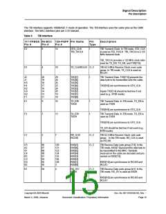
B3
C3
D3
B2
91
93
92
95
125
126
128
3
RXD[3]/RD[3]
RXD[2]/RD[2]
RXD[1]/RD[1]
RXD[0]/RD[0]
O, Z
RGMII Receive Data. In RGMII mode,
RXD[3:0] are used as RD[3:0]. In RGMII
mode, RXD[3:0] run at double data rate with
bits [3:0] presented on the rising edge of
RX_CLK, and bits [7:4] presented on the fall-
ing edge of RX_CLK. In this mode, RXD[7:4]
are ignored.
In RGMII 10/100BASE-T modes, the receive
data nibble is presented on RXD[3:0] on the
rising edge of RX_CLK.
RXD[3:0] are synchronous to RX_CLK.
Copyright © 2009 Marvell
March 4, 2009, Advance
Doc. No. MV-S105540-00, Rev. --
Document Classification: Proprietary Information
Page 17

 MARVELL [ MARVELL TECHNOLOGY GROUP LTD. ]