RF POWER MOSFET CONSIDERATIONS
MOSFET CAPACITANCES
cuited or floating should be avoided. These conditions can
result in turn–on of the devices due to voltage build–up on
the input capacitor due to leakage currents or pickup.
Gate Protection — These devices do not have an internal
monolithic zener diode from gate–to–source. If gate protec-
tion is required, an external zener diode is recommended.
Using a resistor to keep the gate–to–source impedance
low also helps damp transients and serves another important
function. Voltage transients on the drain can be coupled to
the gate through the parasitic gate–drain capacitance. If the
gate–to–source impedance and the rate of voltage change
on the drain are both high, then the signal coupled to the gate
may be large enough to exceed the gate–threshold voltage
and turn the device on.
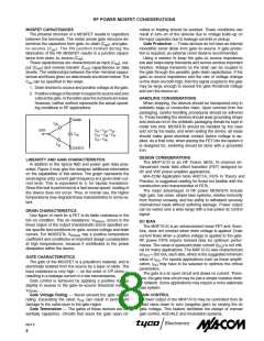
The physical structure of a MOSFET results in capacitors
between the terminals. The metal anode gate structure de-
termines the capacitors from gate–to–drain (Cgd), and gate–
to–source (Cgs). The PN junction formed during the
fabrication of the RF MOSFET results in a junction capaci-
tance from drain–to–source (Cds).
These capacitances are characterized as input (Ciss), out-
put (Coss) and reverse transfer (Crss) capacitances on data
sheets. The relationships between the inter–terminal capaci-
tances and those given on data sheets are shown below. The
C
iss can be specified in two ways:
1. Drain shorted to source and positive voltage at the gate.
2. Positivevoltageofthedraininrespecttosourceandzero
volts at the gate. In the latter case the numbers are lower.
However, neither method represents the actual operat-
ing conditions in RF applications.
HANDLING CONSIDERATIONS
When shipping, the devices should be transported only in
antistatic bags or conductive foam. Upon removal from the
packaging, careful handling procedures should be adhered
to. Those handling the devices should wear grounding straps
and devices not in the antistatic packaging should be kept in
metal tote bins. MOSFETs should be handled by the case
and not by the leads, and when testing the device, all leads
should make good electrical contact before voltage is ap-
plied. As a final note, when placing the FET into the system it
is designed for, soldering should be done with a grounded
iron.
DRAIN
C
gd
GATE
C
= C = C
iss
gd
gs
C
ds
C
= C = C
ds
oss
gd
C
rss
= C
gd
C
gs
SOURCE
DESIGN CONSIDERATIONS
LINEARITY AND GAIN CHARACTERISTICS
The MRF151G is an RF Power, MOS, N–channel en-
hancement mode field–effect transistor (FET) designed for
HF and VHF power amplifier applications.
M/A-COM Application Note AN211A, FETs in Theory and
Practice, is suggested reading for those not familiar with the
construction and characteristics of FETs.
The major advantages of RF power MOSFETs include
high gain, low noise, simple bias systems, relative immunity
from thermal runaway, and the ability to withstand severely
mismatched loads without suffering damage. Power output
can be varied over a wide range with a low power dc control
signal.
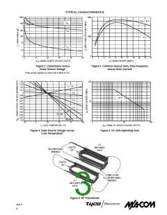
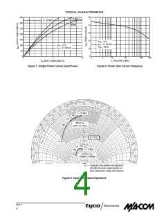
In addition to the typical IMD and power gain data pres-
ented, Figure 3 may give the designer additional information
on the capabilities of this device. The graph represents the
small signal unity current gain frequency at a given drain cur-
rent level. This is equivalent to fT for bipolar transistors.
Since this test is performed at a fast sweep speed, heating of
the device does not occur. Thus, in normal use, the higher
temperatures may degrade these characteristics to some ex-
tent.
DRAIN CHARACTERISTICS
One figure of merit for a FET is its static resistance in the
full–on condition. This on–resistance, VDS(on), occurs in the
linear region of the output characteristic and is specified un-
der specific test conditions for gate–source voltage and drain
current. For MOSFETs, VDS(on) has a positive temperature
coefficient and constitutes an important design consideration
at high temperatures, because it contributes to the power
dissipation within the device.
DC BIAS
The MRF151G is an enhancement mode FET and, there-
fore, does not conduct when drain voltage is applied. Drain
current flows when a positive voltage is applied to the gate.
RF power FETs require forward bias for optimum perfor-
mance. The value of quiescent drain current (IDQ) is not criti-
cal for many applications. The MRF151G was characterized
at IDQ = 250 mA, each side, which is the suggested minimum
value of IDQ. For special applications such as linear amplifi-
cation, IDQ may have to be selected to optimize the critical
parameters.
GATE CHARACTERISTICS
The gate of the MOSFET is a polysilicon material, and is
electrically isolated from the source by a layer of oxide. The
input resistance is very high — on the order of 109 ohms —
resulting in a leakage current of a few nanoamperes.
Gate control is achieved by applying a positive voltage
slightly in excess of the gate–to–source threshold voltage,
The gate is a dc open circuit and draws no current. There-
fore, the gate bias circuit may be just a simple resistive divid-
er network. Some applications may require a more elaborate
bias system.
VGS(th)
.
Gate Voltage Rating — Never exceed the gate voltage
rating. Exceeding the rated VGS can result in permanent
damage to the oxide layer in the gate region.
Gate Termination — The gates of these devices are es-
sentially capacitors. Circuits that leave the gate open–cir-
GAIN CONTROL
Power output of the MRF151G may be controlled from its
rated value down to zero (negative gain) by varying the dc
gate voltage. This feature facilitates the design of manual
gain control, AGC/ALC and modulation systems.
REV 9
8

 TE [ TE CONNECTIVITY ]