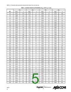
ELECTRICAL CHARACTERISTICS (T = 25°C unless otherwise noted.)
C
Characteristic
Symbol
Min
Typ
Max
Unit
OFF CHARACTERISTICS (Each Side)
Drain–Source Breakdown Voltage (V = 0, I = 100 mA)
V
(BR)DSS
125
—
—
—
—
—
Vdc
mAdc
µAdc
GS
D
Zero Gate Voltage Drain Current (V = 50 V, V = 0)
I
5.0
1.0
DS
GS
DSS
GSS
Gate–Body Leakage Current (V = 20 V, V = 0)
I
—
GS
DS
ON CHARACTERISTICS (Each Side)
Gate Threshold Voltage (V = 10 V, I = 100 mA)
V
1.0
1.0
5.0
3.0
3.0
7.0
5.0
5.0
—
Vdc
Vdc
DS
D
GS(th)
Drain–Source On–Voltage (V = 10 V, I = 10 A)
V
DS(on)
GS
D
Forward Transconductance (V = 10 V, I = 5.0 A)
g
fs
mhos
DS
D
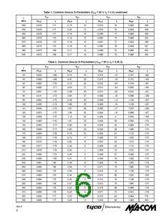
DYNAMIC CHARACTERISTICS (Each Side)
Input Capacitance (V = 50 V, V = 0, f = 1.0 MHz)
C
—
—
—
350
220
15
—
—
—
pF
pF
pF
DS
GS
iss
Output Capacitance (V = 50 V, V = 0, f = 1.0 MHz)
C
oss
DS
GS
Reverse Transfer Capacitance (V = 50 V, V = 0, f = 1.0 MHz)
C
rss
DS
GS
FUNCTIONAL TESTS
Common Source Amplifier Power Gain
G
14
50
16
55
—
—
dB
%
ps
(V = 50 V, P = 300 W, I = 500 mA, f = 175 MHz)
DD
out
DQ
Drain Efficiency
η
(V = 50 V, P = 300 W, f = 175 MHz, I (Max) = 11 A)
DD
out
D
Load Mismatch
ψ
(V = 50 V, P = 300 W, I = 500 mA,
No Degradation in Output Power
DD
out
DQ
VSWR 5:1 at all Phase Angles)
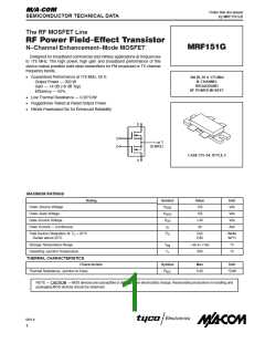
R1
L2
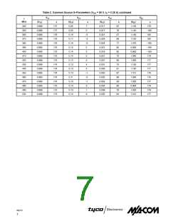
+
+
C4
C5
C9 C10
50 V
–
BIAS 0–6 V
–
C11
C12
L1
D.U.T.
T2
R2
C1
OUTPUT
T1
INPUT
C6
C2
C3
C7
C8
R1 — 100 Ohms, 1/2 W
R2 — 1.0 kOhm, 1/2 W
C1 — Arco 424
C2 — Arco 404
C3, C4, C7, C8, C9 — 1000 pF Chip
C5, C10 — 0.1 µF Chip
C6 — 330 pF Chip
C11 — 0.47 µF Ceramic Chip, Kemet 1215 or
C11 — Equivalent (100 V)
T1 — 9:1 RF Transformer. Can be made of 15–18 Ohms
T1 — Semirigid Co–Ax, 62–90 Mils O.D.
T2 — 1:4 RF Transformer. Can be made of 16–18 Ohms
T2 — Semirigid Co–Ax, 70–90 Mils O.D.
Board Material — 0.062″ Fiberglass (G10),
1 oz. Copper Clad, 2 Sides, ε = 5.0
r
C12 — Arco 422
L1 — 10 Turns AWG #18 Enameled Wire,
L1 — Close Wound, 1/4″ I.D.
L2 — Ferrite Beads of Suitable Material for
L2 — 1.5–2.0 µH Total Inductance
NOTE: For stability, the input transformer T1 must be loaded
NOTE: with ferrite toroids or beads to increase the common
NOTE: mode inductance. For operation below 100 MHz. The
NOTE: same is required for the output transformer.
Unless Otherwise Noted, All Chip Capacitors are ATC Type 100 or
Equivalent.
See Figure 6 for construction details of T1 and T2.
Figure 1. 175 MHz Test Circuit
REV 9
2

 TE [ TE CONNECTIVITY ]