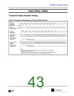
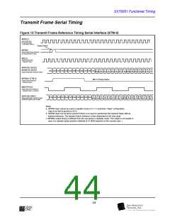
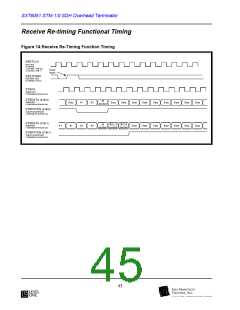
SXT6051 STM-1/0 SDH Overhead Terminator
bytes (But not the stuffed column). In
STM-0 this output is tied High
long and cover the J1 time slot. (See
timing for further details)
MTBTUGEN3 A High indicates the location of TUG3
#3, plus the position of the VC-4 POH
bytes (But not the stuffed column). In
STM-0 this output is tied High.
Note that MMFRMI input pin is not
used and is tied to ground.
MTBJ0J1EN
This input indicates J0 and J1 bytes’
locations
on
MTBDATA<7:0>.
MTBJ0J1EN can be configured via
register 71H in two ways:
Multiplexer Telecom Bus ADM
Mode
In this mode, the Telecom Bus is a co-directional interface.
This means the SXT6051 receives the timing references
(clock and signals) and the associated data.
•A single pulse at J0 position and a
single pulse at J1 position indi-
cates when the frame and the
payload starts.
The signals for this mode are:
•A single pulse at J0 position, a sin-
gle pulse at J1 position and a dou-
ble pulse on J1 every four frames
indicating a multiframe.
MTBDATA<7:0> Identical to the Terminal mode.
MTBPAR
MTBCKO
MTBCKI
Identical to the Terminal mode.
Output is tri-stated (not used).
MTBTUGEN1
MTBTUGEN2
MTBTUGEN3
Outputs are tri-stated (not used).
Outputs are tri-stated (not used).
Outputs are tri-stated (not used).
This input is the Telecom Bus byte
clock (6.48 MHz in STM0 and 19.44
MHz in STM1 mode). It can be asyn-
chronous to the transmit reference
clock input.
Demultiplexer Telecom Bus
(Terminal or ADM) Mode
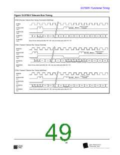
Note that the incoming data (MTB-
PAR and MTBDATA<7:0>) and
Telecom bus Timing references
(MTBH4EN, MTBPAYEN, and
MTBJ0J1EN) are internally clocked
by the falling edge of MTBCKI (see
Telecom bus timings).
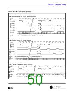
Note on Telecom Bus
Timing Reference
All transitions of the Telecom bus Timing
references (DTBH4EN, DTBPAYEN, DTBJ0EN
and DTBTUGEN) and the outgoing data
(DTBPAR and DTBDATA<7:0>) are clocked by
the rising edge of DTBCK (see Telecom bus
timings).
MTBPAYEN
MTBH4EN
A High on this input indicates the
location of the VC-4 (STM-1 mode) or
the VC-3 with two stuffed columns
(STM-0 mode). A Low indicates the
location of the SOH bytes and the AU
Pointers bytes.
The signals for this mode are:
DTBDATA<7:0>Byte wide data output with either STM-
1 or STM-0 frame structure depending
on STMMODE selection.
This input indicates the multiframe
start position. This input is not used if
MTBJ0J1EN is configured to support
the “framing-multiframing indication”
(see register 71H<7>). When used,
this signal must be High one frame
every fourth frame. It is possible to use
a pulse as an indicator. As a minimum,
this pulse has to be one clock cycle
DTBPAR
DTBDATA<7:0> parity check. An odd
parity bit calculation accompanies each
data byte input (including the bytes fill-
ing the SOH, AUP and HPOH loca-
tions).
47

 LevelOne [ LEVEL ONE ]