LTC1699 Series
U
U
U
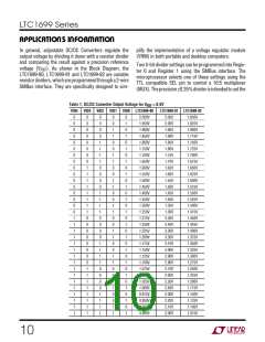
PI FU CTIO S
Note: Pin numbers apply to 16-lead SSOP packages.
NC (Pin 7): Not connected.
SEL (Pin 1): Register Select Input. A TTL compatible logic
input pin that is used to select 1 of 2 resistor divider
settings. SEL selects the setting in Register 0 if pulled low
and the setting in Register 1 if pulled high.
CPU_ON (Pin 8): CPU DC/DC Converter Control. Open
drainoutput,usuallyconnectedtotheRUN/SSpinofaDC/
DC converter that generates the CPU core supply. It pulls
low to shut down the converter or becomes a high imped-
ance state to allow the converter to soft-start.
NC (Pin 2): Not connected.
IO_ON (Pin 9): I/O DC/DC Converter Control. Open drain
output, normally connected to the RUN/SS pin of the DC/
DC converter that generates the I/O supply. It pulls low to
shut down the converter or becomes a high impedance
state to allow the converter to soft-start.
SDA (Pin 3): SMBus Data Input/Output. SDA is a high
impedance input when address, command or data bits are
shifted in. It is an open drain, N-channel output when
acknowledging or sending data back to the microproces-
sor during read-back. It requires a pull-up resistor or
current source to VCC.
CLK_ON (Pin 10): Clock DC/DC Converter Control. Open
drain output, optionally connected to the RUN/SS pin of
the DC/DC converter that generates the supply for the
clock buffer. It pulls low to shut down the converter or
becomes a high impedance state to allow the converter to
soft-start.
SCL (Pin 4): SMBus Clock Input. Data at the SDA pin is
latchedintotheLTC1699attherisingedgeoftheclockand
is shifted out of the SDA pin at the falling edge of the clock.
SCL is a high impedance input pin. It is driven by the open
collector output of a microprocessor and requires a pull-
up resistor or current source to VCC.
NC (Pin 11): Not connected.
VRON (Pin 5): Global Control Input. This TTL compatible
input pin is pulled up internally by a 2.5µA current source.
Pulling VRON low forces the open drain output pins
(CPU_ON,IO_ON,CLK_ONandPGOOD)topulltoground.
If the LTC1699-80, LTC1699-81 or LTC1699-82 is pro-
grammedtoturnonDC/DCconverters, pullingVRONhigh
three-states the CPU_ON, IO_ON and CLK_ON pins and
allows the DC/DC converters to soft-start.
SENSE (Pin 12): Sense Input. Upper terminal of the
resistor divider that is connected directly to the output
voltage being regulated.
FB (Pin 13): Feedback Input. Center tap of the divider that
isconnectedtothefeedbackpinofanLTC0.8Vreferenced
DC/DC converter.
GND(Pin14):Ground.Connecttoregulatorsignalground.
GND (Pin 15): Divider Ground. Short to Pin 14.
PGOOD (Pin 6): Power Good Output. This open drain
output is pulled low for 50µs each time the LTC1699-80,
LTC1699-81 or LTC1699-82 turns on the DC/DC convert-
ers or SEL is toggled to select a new code. PGOOD may be
connected to the FCB input of an LTC DC/DC converter to
force the converter into continuous mode operation. This
reduces the time needed for the converter output to settle
to a lower output voltage under light load conditions if the
SEL pin is toggled.
VCC (Pin 16): Positive Supply. 2.7V ≤ VCC ≤ 5.5V. Bypass
this pin to ground with a 0.1µF ceramic capacitor.
6

 Linear [ Linear ]