LTC1699 Series
W W U W
ABSOLUTE AXI U RATI GS
(Note 1)
Supply Voltage (VCC) ................................................. 7V
All Pins ........................................................–0.3V to 7V
Operating Temperature
Storage Temperature ...................... -65°C ≤ TA ≤ 150°C
Lead Temperature (Soldering, 10 sec).................. 300°C
Range (Note 2) ................................ –40°C ≤ TA ≤ 85°C
Junction Temperature........................................... 125°C
U
W
U
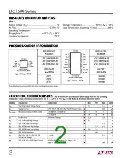
PACKAGE/ORDER I FOR ATIO
TOP VIEW
ORDER PART
NUMBER
ORDER PART
1
2
3
4
5
6
7
8
V
CC
16
15
14
13
12
11
10
9
SEL
NC
NUMBER
GND
LTC1699EMS8-80
LTC1699EMS8-81
LTC1699EMS8-82
LTC1699EGN-80
LTC1699EGN-81
LTC1699EGN-82
TOP VIEW
GND
SDA
SEL
SDA
SCL
1
2
3
4
8 V
CC
7 GND
6 FB
FB
SCL
SENSE
NC
VRON
PGOOD
NC
5 SENSE
PGOOD
MS8 PACKAGE
8-LEAD PLASTIC MSOP
MS8 PART
MARKING
GN PART
MARKING
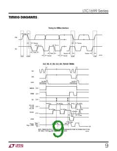
CLK_ON
IO_ON
CPU_ON
TJMAX = 125°C, θJA = 200°C/W
GN PACKAGE
16-LEAD PLASTIC SSOP
LTPV
LTPW
LTTB
169980
169981
169982
TJMAX = 125°C, θJA = 130°C/W
Consult factory for parts specified with wider operating temperature ranges.
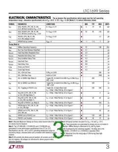
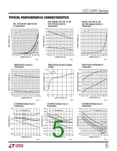
ELECTRICAL CHARACTERISTICS
The ● denotes the specifications which apply over the full operating
temperature range, otherwise specifications are at TA = 25°C. 2.7V ≤ VCC ≤ 5.5V (Notes 3, 4) unless otherwise stated.
SYMBOL
PARAMETER
CONDITIONS
MIN
TYP
MAX
5.5
UNITS
V
V
Operating Supply Voltage Range
Supply Current
2.7
CC
I
CPU_ON, IO_ON, CLK_ON, PGOOD Pins Are Open
LTC1699-80, LTC1699-82
LTC1699-81
●
●
●
●
●
●
350
13
µA
kΩ
kΩ
%
CC
R
Resistance between SENSE and FB
7
14
10
20
FB-SENSE
26
DE
Divider Error
All Divider Settings
–0.35
2.1
0.35
V
V
V
V
V
V
SCL, SDA Input High Voltage
SCL, SDA Input Low Voltage
SEL, VRON Input High Voltage
SEL, VRON Input Low Voltage
SEL, VRON Hysteresis
V
IH
0.8
2.0
V
IL
1.3
1.3
V
IH
●
●
0.8
V
IL
±50
mV
V
HYST
OL
SDA, CPU_ON, IO_ON, CLK_ON
Output Low Voltage
I = 3mA
0.4
I
SCL, SDA, SEL, VRON Input Current
SDA Not Acknowledging, 0 ≤ V ≤ 5.5V,
PIN
IN
V
= 5.5V for VRON only
●
±10
µA
PIN
2

 Linear [ Linear ]