LTC1699 Series
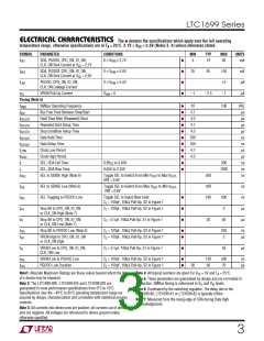
ELECTRICAL CHARACTERISTICS
The ● denotes the specifications which apply over the full operating
temperature range, otherwise specifications are at TA = 25°C. 2.7V ≤ VCC ≤ 5.5V (Notes 3, 4) unless otherwise stated.
SYMBOL
PARAMETER
CONDITIONS
0 ≤ V ≤ 2.7V
MIN
TYP
MAX
UNITS
I
I
I
I
SDA, PGOOD, CPU_ON, IO_ON,
CLK_ON Sink Current at V = 2.7V
●
●
●
●
5
19
60
mA
SK1
SK2
LKG
PU
PIN
CC
SDA, PGOOD, CPU_ON, IO_ON,
CLK_ON Sink Current at V = 5.5V
0 ≤ V ≤ 5.5V
35
65
150
±2
mA
µA
µA
PIN
CC
PGOOD, CPU_ON, IO_ON,
CLK_ON Leakage Current
0 ≤ V ≤ 5.5V
PIN
VRON Pull-Up Current
V
= 0
–1
–2.5
–7
PIN
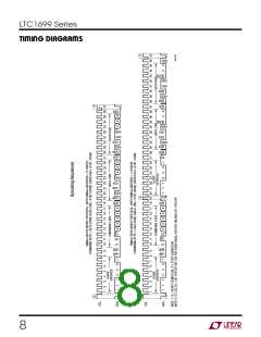
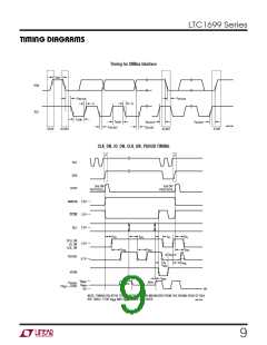
Timing (Note 5)
f
t
t
t
t
t
t
t
t
t
t
t
SMBus Operating Frequency
Bus Free Time Between Stop/Start
Hold Time After (Repeated) Start
Repeated Start Setup Time
Stop Condition Setup Time
Data Hold Time
●
●
●
●
●
●
●
●
●
●
●
10
4.7
4.0
4.7
4.0
300
250
4.7
4.0
100
KHz
µs
µs
µs
µs
ns
ns
µs
µs
ns
ns
ns
SMB
BUF
HD:STA
SU:STA
SU:STO
HD:DAT
SU:DAT
LOW
HIGH
f
Data Setup Time
Clock Low Period
Clock High Period
SCL, SDA Fall Time
0.9V to 0.65V
300
CC
SCL, SDA Rise Time
0.65V to 2.25V
1000
r
SEL to SENSE High (Note 6)
Toggle SEL to Switch from Min V
VFB = 0.8V
to Max V
to Min V
,
,
500
500
160
SSH
OUT
OUT
t
t
t
t
SEL to SENSE Low (Note 6)
SEL Toggling to PGOOD Low
Toggle SEL to Switch from Max V
VFB = 0.8V
ns
ns
µs
µs
SSL
SPL
PH
OUT
OUT
Toggle SEL to Select New Code
C = 100pF, 10kΩ Pull-Up, S2 in Figure 1
L
●
●
●
500
2
Stop Bit to CPU_ON, IO_ON
or CLK_ON High (Note 7)
C = 100pF, 10kΩ Pull-Up, S2 in Figure 1
L
Stop Bit to CPU_ON, IO_ON
or CLK_ON Low (Note 7)
C = 0.1µF, 10kΩ Pull-Up, S1 in Figure 1
L
20
50
PL
t
t
Stop Bit to PGOOD Low (Note 6)
C = 100pF, 10kΩ Pull-Up, S2 in Figure 1
●
●
250
2
ns
PPL
VH
L
VRON High to CPU_ON, IO_ON
or CLK_ON High
C = 100pF, 10kΩ Pull-Up, S2 in Figure 1
L
µs
t
VRON Low to CPU_ON, IO_ON,
CLK_ON Low
C = 0.1µF, 10kΩ Pull-Up, S1 in Figure 1
L
●
50
µs
VL
t
t
VRON Low to PGOOD Low
PGOOD Low Duration
C = 100pF, 10kΩ Pull-Up, S2 in Figure 1
●
●
130
50
500
70
ns
VPL
PGL
L
C = 100pF, 10kΩ Pull-Up, S2 in Figure 1
L
30
µs
Note1: Absolute Maximum Ratings are those values beyond which the life
Note 4: All typical numbers are given for V = 5V and T = 25°C.
CC A
of a device may be impaired.
Note 5: These parameters are guaranteed by design and are not tested in
production. SMBus timing is referenced to V and V levels.
Note 6: Dominated by the switching regulator. The delay due to the
LTC1699-80, LTC1699-81 or LTC1699-82 is typically 500ns.
Note 7: Measured from the rising edge of SDA during Data High
Note 2: The LTC1699-80E, LTC1699-81E and LTC1699-82E are
guaranteed to meet performance specifications from 0°C to 70°C.
Specifications over the –40°C to 85°C operating temperature range are
assured by design, characterization and correlation with statistical process
controls.
Note 3: All currents into device pins are positive; all currents out of device
pins are negative. All voltages are referenced to device ground unless
otherwise specified.
IL
IH
acknowledgement.
3

 Linear [ Linear ]