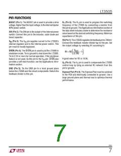
LT3505
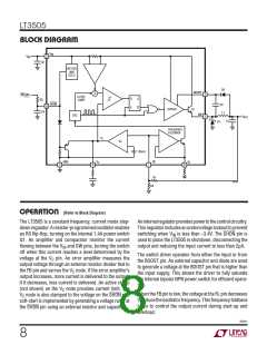
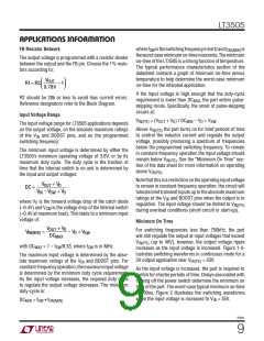
APPLICATIONS INFORMATION
When the input voltage is below 16V, the zener diode
path conducts no current and the current flowing out
of the RT pin (and through R4) is nominally 0.5V/20k =
25µA, which programs a 2.2MHz switching frequency.
As the input voltage is increased above 16V, the zener
diode begins to conduct and gradually reduces the cur-
rent flowing out of the RT pin. This mechanism reduces
the switching frequency as the input voltage is increased
above 16V (up to 36V) to ensure that the part constantly
operates in continuous mode without skipping pulses,
thereby preventing the excessive die temperature rise
encountered in pulse-skipping mode.
Finite transistor bandwidth limits the speed at which the
power switch can be turned on and off, effectively setting
theminimumon-timeoftheLT3505.Foragivenoutputvolt-
age,theminimumon-timedeterminesthemaximuminput
voltage to remain in continuous mode operation, VIN(PS)
.
See the “Input Voltage Range” section of the datasheet for
more information on determining VIN(PS). For switching
frequencies below 750kHz, operation above VIN(PS) (up
to 40V) is safe provided that the system will tolerate the
pulse-skipping behavior outlined in the “Minimum On
Time” section of the datasheet. At switching frequencies
exceeding 750kHz, edge loss limits operation to input
voltages below VIN(PS)
.
Although the circuit can be operated indefinitely above
VZENER, this frequency foldback method is intended to
protect circuits during temporary periods of high input
voltage. For example, in many automotive systems, the
normal operating input range might be 9V to 16V, and
the LT3505 can be programmed to operate above the
AM band (>1.8MHz). At the same time, the circuit must
be able to withstand higher input voltages due to load
dump or double-battery jump starts. During these brief
periods, it is usually acceptable to switch at a frequency
within the AM band.
Finite transition time results in a small amount of power
dissipation each time the power switch turns on and off
(edge loss). Edge loss increases with frequency, switch
current, and input voltage.
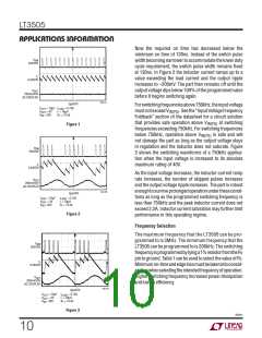
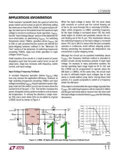
Input Voltage Frequency Foldback
In constant frequency operation (below VIN(PS)) edge
loss only reduces the application efficiency. However, at
high switching frequencies exceeding 750kHz and input
voltagesexceedingVIN(PS),thepartoperatesinpulse-skip-
ping mode and the switch current can increase above the
current limit of the part, 1.75A. This further increases the
power dissipated during switch transitions and increases
die temperature. To remedy the situation a single resis-
tor (R5) and a zener diode (D3) can be added to a typical
LT3505 circuit as shown in Figure 4.
Iftheoutputisshortedwhiletheinputvoltageisgreaterthan
VZENER, the switching frequency will be reduced to 30kHz
and the part will not be able to recover from the short until
theinputvoltageisreducedbelowVZENER(seethefollowing
discussion).
2.50
D2
1N4148
2.25
V
V
OUT
IN
V
BOOST
SW
IN
5V
6.7V TO 36V
2.00
C3
0.1µF
1.75
ON OFF
SHDN
L1
C5
22pF
R1
1.50
LT3505
GND
6.8µH
61.9k
D3
1.25
16V
FB
BZT52C16T
1.00
C1
10µF
D1
R2
11.5k
R5
806k
R
T
V
C
MBRM140
0.75
0.50
0.25
0
Switching
Frequency
R4
R3
Maximum
20.0k
100k
Load Current
C2
1µF
C4
22pF
0
30 35
5
10 15
20
Input Voltage [V]
25
40
LTC3505 • F04b
3505 F04
Figure 4. 2.2MHz, 5V Application with Input Voltage Frequency Foldback Circuit
3505fc
11

 Linear [ Linear ]