LT3505
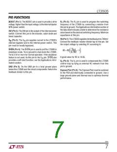
PIN FUNCTIONS
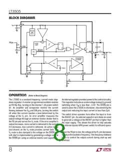
BOOST (Pin 1): The BOOST pin is used to provide a drive
voltage,higherthantheinputvoltage,totheinternalbipolar
NPN power switch.
RT (Pin 6): The RT pin is used to program the switching
frequency of the LT3505 by connecting a resistor from
thispintoground.TheApplicationsInformationsectionof
the data sheet includes a table to determine the resistance
value based on the desired switching frequency. Minimize
capacitance at this pin.
SW (Pin 2): The SW pin is the output of the internal power
switch. Connect this pin to the inductor, catch diode and
boost capacitor.
FB(Pin7):TheLT3505regulatesitsfeedbackpinto780mV.
Connect the feedback resistor divider tap to this pin. Set
the output voltage by selecting R1 according to:
VIN (Pin 3): The VIN pin supplies current to the LT3505’s
internal regulator and to the internal power switch. This
pin must be locally bypassed.
VOUT
0.78V
SHDN (Pin 4): The SHDN pin is used to put the LT3505 in
shutdown mode. Tie to ground to shut down the LT3505.
Tie to 2.3V or more for normal operation. If the shutdown
feature is not used, tie this pin to the VIN pin. SHDN also
provides a soft-start function; see the Applications Infor-
mation section.
R1= R2
– 1
A good value for R2 is 10.0k.
VC (Pin 8): The VC pin is used to compensate the LT3505
control loop by tying an external RC network from this
pin to ground.
GND (Pin 5): Tie the GND pin to a local ground plane
below the LT3505 and the circuit components. Return the
feedback divider to this pin.
Exposed Pad (Pin 9): The Exposed Pad must be soldered
to the PCB and electrically connected to ground. Use a
large ground plane and thermal vias to optimize thermal
performance.
3505fc
7

 Linear [ Linear ]