LT3505
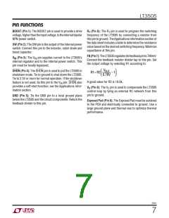
APPLICATIONS INFORMATION
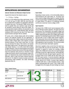
FB Resistor Network
wherefSWistheswitchingfrequencyinhertzandtON(MIN)is
theworst-caseminimumon-timeinseconds.Theminimum
on-time of the LT3505 is a strong function of temperature.
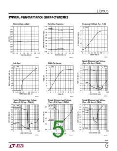
The typical performance characteristics section of the
datasheet contains a graph of minimum on-time versus
temperature to help determine the worst-case minimum
on-time for the intended application.
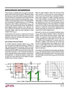
The output voltage is programmed with a resistor divider
between the output and the FB pin. Choose the 1% resis-
tors according to:
VOUT
0.78V
R1= R2
– 1
If the input voltage is high enough that the duty-cycle
requirement is lower than DCMIN, the part enters pulse-
skipping mode. Specifically, the onset of pulse-skipping
occurs at:
R2 should be 20k or less to avoid bias current errors.
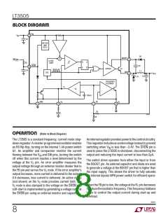
Reference designators refer to the Block Diagram.
Input Voltage Range
VIN(PS) = (VOUT + VD) / DCMIN – VD + VSW
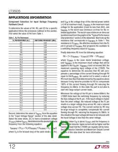
The input voltage range for LT3505 applications depends
on the output voltage, on the absolute maximum ratings
of the VIN and BOOST pins, and on the programmed
switching frequency.
Above VIN(PS) the part turns on for brief periods of time
to control the inductor current and regulate the output
voltage, possibly producing a spectrum of frequencies
below the programmed switching frequency. To remain
in constant-frequency operation the input voltage should
remain below VIN(PS). See the “Minimum On Time” sec-
tion of the data sheet for more information on operating
The minimum input voltage is determined by either the
LT3505’s minimum operating voltage of 3.6V, or by its
maximum duty cycle. The duty cycle is the fraction of
time that the internal switch is on and is determined by
the input and output voltages:
above VIN(PS)
.
Notethatthisisarestrictionontheoperatinginputvoltage
to remain in constant-frequency operation; the circuit will
tolerate brief transient inputs up to the absolute maximum
ratings of the VIN and BOOST pins when the output is in
regulation. The input voltage should be limited to VIN(PS)
during overload conditions (short-circuit or start-up).
VOUT + VD
DC =
V – VSW + VD
IN
where VD is the forward voltage drop of the catch diode
(~0.4V) and VSW is the voltage drop of the internal switch
(~0.4V at maximum load). This leads to a minimum input
voltage of:
Minimum On Time
VOUT + VD
DCMAX
For switching frequencies less than 750kHz, the part
will still regulate the output at input voltages that exceed
VIN(PS) (up to 40V), however, the output voltage ripple
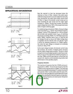
increases as the input voltage is increased. Figure 1 il-
lustrates switching waveforms in continuous mode for a
3V output application near VIN(PS) = 33V.
V
=
– VD + VSW
IN(MIN)
with DCMAX = 1 – fSW/8.33, where fSW is in MHz.
The maximum input voltage is determined by the abso-
lute maximum ratings of the VIN and BOOST pins. For
constant-frequencyoperation,themaximuminputvoltage
is determined by the minimum duty cycle requirement.
As the input voltage increases, the required duty cycle
to regulate the output voltage decreases. The minimum
duty-cycle is:
As the input voltage is increased, the part is required to
switch for shorter periods of time. Delays associated with
turning off the power switch determine the minimum on
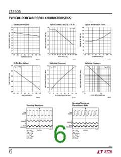
time of the part. The worst-case typical minimum on-time
is 130ns. Figure 2 illustrates the switching waveforms
when the input voltage is increased to VIN = 35V.
DCMIN = fSW
t
ON(MIN)
•
3505fc
9

 Linear [ Linear ]