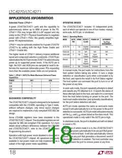
LTC4270/LTC4271
PIN FUNCTIONS
LTC4270
AGND (Pin 34): Analog Ground. Connect AGND to the
return for the V supply.
EE
SENSEn (Pins 1, 4, 8, 11, 15, 18, 21, 24, 30, 33, 37,
40): Port n Current Sense Input. SENSEn monitors the
external MOSFET current via a 0.5Ω or 0.25Ω sense
V (Pins 41, 51, 52): Main PoE Supply Input. Connect to
EE
a –45V to –57V supply, relative to AGND. Voltage depends
++
resistor between SENSEn and V . Whenever the voltage
on PSE type (Type 1, Type 2 or LTPoE .)
EE
acrossthesenseresistorexceedstheovercurrentdetection
DNA (Pin 47): Data Transceiver Negative Input Output
(Analog). Connect to DND through a data transformer.
threshold V , the current limit fault timer counts up. If
CUT
the voltage across the sense resistor reaches the current
DPA (Pin 48): Data Transceiver Positive Input Output
(Analog). Connect to DPD through a data transformer.
limit threshold V , the GATEn pin voltage is lowered to
LIM
maintain constant current in the external MOSFET. See
Applications Information for further details. If the port is
CNA (Pin 49): Clock Transceiver Negative Input Output
(Analog). Connect to CND through a data transformer.
unused, the SENSEn pin must be tied to V .
EE
GATEn (Pins 2, 5, 9, 12, 16, 19, 22, 25, 29, 32, 36, 39):
Port n Gate Drive. GATEn should be connected to the gate
of the external MOSFET for port n. When the MOSFET is
turned on, the gate voltage is driven to 13V (typ) above
CPA (Pin 50): Clock Transceiver Positive Input Output
(Analog). Connect to CPD through a data transformer.
VSSK(ExposedPadPin53):KelvinSensetoV . Connect
EE
to sense resistor common node. Do not connect directly
V . During a current limit condition, the voltage at GATEn
EE
to V plane. See Layout Guide.
EE
will be reduced to maintain constant current through the
externalMOSFET. Ifthefaulttimerexpires, GATEnispulled
down, turning the MOSFET off and recording a port fault
event. If the port is unused, float the GATEn pin.
Common Pins
NC, DNC (LTC4271 Pins 7,13; LTC4270 Pins 42, 43, 44,
45, 46): All pins identified with “NC” or “DNC” must be
left unconnected.
OUTn (Pins 3, 6, 10, 13, 17, 20, 23, 26, 28, 31, 35, 38):
Port n Output Voltage Monitor. OUTn should be connected
to the output port. A current limit foldback circuit limits
the power dissipation in the external MOSFET by reducing
the current limit threshold when the drain-to-source volt-
age exceeds 10V. The port n Power Good bit is set when
LTC4271
AD0(Pin1):AddressBit0.Tietheaddresspinshighorlow
2
to set the starting I C serial address to which the LTC4271
responds. The chip will respond to this address plus the
next two incremental addresses. The base address of the
the voltage from OUTn to V drops below 2.4V (typ). A
EE
500k resistor is connected internally from OUTn to AGND
when the port is idle. If the port is unused, the OUTn pin
must be floated.
first four ports will be (A 10A A A A )b. The second and
6 3 2 1 0
third groups of four ports will respond at the next two
logical addresses. Internally pulled up to V .
DD
CAP2 (Pin 7): Analog Internal 4.3V Power Supply Bypass
AD1 (Pin 2): Address Bit 1. See AD0.
AD2 (Pin 3): Address Bit 2. See AD0.
AD3 (Pin 4): Address Bit 3. See AD0.
AD6 (Pin 5): Address Bit 6. See AD0.
Capacitor. Connect 0.1μF ceramic cap to V .
EE
XIO0(Pin14):GeneralPurposeDigitalInputOutput.Logic
signal between V and V + 4.3V. Internal pull up.
EE
EE
XIO1(Pin27):GeneralPurposeDigitalInputOutput.Logic
signal between V and V + 4.3V. Internal pull up.
MID(Pin6):MidspanModeInput.Whenhigh,theLTC4271
actsasamidspandevice. InternallypulleddowntoDGND.
EE
EE
42701f
14

 Linear [ Linear ]