LTC2640
OPERATION
Serial Interface
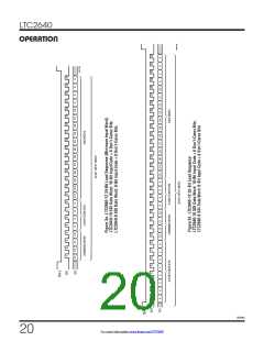
transferred to the device first, followed by the 24-bit se-
quence described. Figure 3b shows the 32-bit sequence.
The CS/LD input is level triggered. When this input is
taken low, it acts as a chip-select signal, enabling the
SDI and SCK buffers and the input shift register. Data
(SDI input) is transferred at the next 24 rising SCK edges.
The 4-bit command, C3-C0, is loaded first, followed by
4 don’t-cares bits, and finally the 16-bit data word. The
data word comprises the 12-, 10- or 8-bit input code, or-
dered MSB-to-LSB, followed by 4, 6 or 8 don’t-cares bits
(LTC2640-12, LTC2640-10 and LTC2640-8 respectively;
see Figure 2). Data can only be transferred to the device
when the CS/LD signal is low, beginning on the first rising
edge of SCK. SCK may be high or low at the falling edge
of CS/LD. The rising edge of CS/LD ends the data transfer
and causes the device to execute the command specified
in the 24-bit input sequence. The complete sequence is
shown in Figure 3a.
The 16-bit data word is ignored for all commands that do
not include a Write operation.
Reference Modes
Forapplicationswhereanaccurateexternalreferenceisnot
available, the LTC2640 has a user-selectable, integrated
reference. The LTC2640-LM/LTC2640-LZ provide a full-
scale output of 2.5V. The LTC2640-HM/LTC2640-HZ
provideafull-scaleoutputof4.096V.Theinternalreference
can be useful in applications where the supply voltage is
poorlyregulated. InternalReferencemodecanbeselected
by using command 0110, and is the power-on default for
LTC2640-HZ/LTC2640-LZ, as well as for LTC2640-HM/
LTC2640-LM when REF_SEL is tied high.
The 10ppm/°C, 1.25V (LTC2640-LM/LTC2640-LZ) or
2.048V (LTC2640-HM/LTC2640-HZ) internal reference
is available at the REF pin. Adding bypass capacitance
to the REF pin will improve noise performance; 0.33µF
is recommended, and up to 10µF can be driven without
oscillation. This output must be buffered when driving an
external DC load current.
The command (C3-C0) assignments are shown in Table 1.
The first three commands in the table consist of write and
update operations. A Write operation loads a 16-bit data
word from the 24-bit shift register into the input register.
In an Update operation, the input register is copied to the
DAC register and converted to an analog voltage at the
DAC output. Write to and Update combines the first two
commands. The Update operation also powers up the
DAC if it had been in power-down mode. The data path
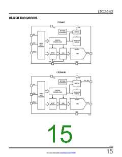
and registers are shown in the Block Diagram.
Alternatively, the DAC can operate in External Reference
modeusingcommand0111.Inthismode,aninputvoltage
supplied externally to the REF pin provides the reference
(0V≤V ≤V )andthesupplycurrentisreduced.External
REF
CC
Table 1. Command Codes
COMMAND*
Referencemodeisthepower-ondefaultforLTC2640-HM/
LTC2640-LM when REF_SEL is tied low.
C3
0
C2
0
C1 C0
The reference mode of LTC2640-HZ/LTC2640-LZ can be
changed only by software command. The same is true for
LTC2640-HM/LTC2640-LM after power-on, after which
the logic state on REF_SEL is ignored.
0
0
1
0
1
1
0
1
1
0
0
1
Write to Input Register
0
0
Update (Power-Up) DAC Register
Write to and Update (Power-Up) DAC Register
Power Down
0
0
0
1
0
1
Select Internal Reference
Power-Down Mode
0
1
Select External Reference
Forpower-constrainedapplications,theLTC2640’spower-
down mode can be used to reduce the supply current
whenever the DAC output is not needed. When in power-
down, the buffer amplifier, bias circuit, and reference
circuit are disabled and draw essentially zero current. The
DAC output is put into a HIGH-impedance state, and the
output pin is passively pulled to ground through a 200k
*Command codes not shown are reserved and should not be used
While the minimum input sequence is 24-bits, it may
optionally be extended to 32-bits to accommodate micro-
processors that have a minimum word width of 16-bits
(2-bytes). To use the 32-bit width, 8 don’t-cares bits are
2640fd
18
For more information www.linear.com/LTC2640

 Linear [ Linear ]