LTC2640
OPERATION
resistor.InputandDACregistercontentsarenotdisturbed
during power-down.
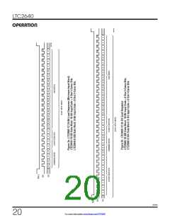
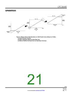
SincetheanalogoutputoftheDACcannotgobelowground,
it may limit the lowest codes, as shown in Figure 4b.
Similarly, limiting can occur near full-scale when the REF
The DAC can be put into power-down mode by using
command 0100. The supply current is reduced to 1.8µA
maximum(CandIgrades)andtheREFpinbecomesHIGH
impedance (typically > 1GΩ).
pin is tied to V . If V = V and the DAC full-scale error
CC
REF
CC
(FSE) is positive, the output for the highest codes limits
at V , as shown in Figure 4c. No full-scale limiting can
CC
occur if V is less than V – FSE.
REF
CC
Normal operation resumes after executing any command
that includes a DAC update, as shown in Table 1. The DAC
is powered up and its voltage output is updated. Normal
settling is delayed while the bias, reference, and ampli-
fier circuits are re-enabled. When the REF pin output is
bypassed to GND with 1nF or less, the power-up delay
time is 20µs for settling to 12-bits. This delay increases
to 200µs for 0.33µF, and 10ms for 10µF.
Offset and linearity are defined and tested over the region
of the DAC transfer function where no output limiting can
occur.
Board Layout
ThePCboardshouldhaveseparateareasfortheanalogand
digital sections of the circuit. A single, solid ground plane
should be used, with analog and digital signals carefully
routed over separate areas of the plane. This keeps digital
signals away from sensitive analog signals and minimizes
the interaction between digital ground currents and the
analog section of the ground plane. The resistance from
the LTC2640 GND pin to the ground plane should be as
low as possible. Resistance here will add directly to the
effective DC output impedance of the device (typically
0.1Ω). Note that the LTC2640 is no more susceptible to
this effect than any other parts of this type; on the con-
trary, it allows layout-based performance improvements
to shine rather than limiting attainable performance with
excessive internal resistance.
Voltage Output
The LTC2640’s integrated rail-to-rail amplifier has guar-
anteed load regulation when sourcing or sinking up to
10mA at 5V, and 5mA at 3V.
Load regulation is a measure of the amplifier’s ability to
maintain the rated voltage accuracy over a wide range of
load current. The measured change in output voltage per
change in forced load current is expressed in LSB/mA.
DC output impedance is equivalent to load regulation, and
may be derived from it by simply calculating a change in
units from LSB/mA to ohms. The amplifier’s DC output
impedance is 0.1Ω when driving a load well away from
the rails.
Another technique for minimizing errors is to use a sepa-
rate power ground return trace on another board layer.
The trace should run between the point where the power
supply is connected to the board and the DAC ground pin.
Thus the DAC ground pin becomes the common point for
analog ground, digital ground, and power ground. When
the LTC2640 is sinking large currents, this current flows
out the ground pin and directly to the power ground trace
without affecting the analog ground plane voltage.
When drawing a load current from either rail, the output
voltage headroom with respect to that rail is limited by
the 50Ω typical channel resistance of the output devices
(e.g., when sinking 1mA, the minimum output voltage is
50Ω • 1mA, or 50mV). See the graph “Headroom at Rails
vs. Output Current” in the Typical Performance Charac-
teristics section.
It is sometimes necessary to interrupt the ground plane
to confine digital ground currents to the digital portion of
the plane. When doing this, make the gap in the plane only
as long as it needs to be to serve its purpose and ensure
that no traces cross over the gap.
The amplifier is stable driving capacitive loads of up to
500pF.
Rail-to-Rail Output Considerations
Inanyrail-to-railvoltageoutputdevice,theoutputislimited
to voltages within the supply range.
2640fd
19
For more information www.linear.com/LTC2640

 Linear [ Linear ]