LTC2640
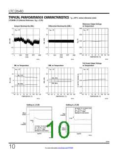
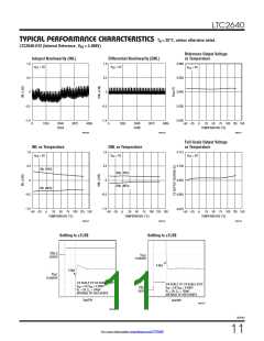
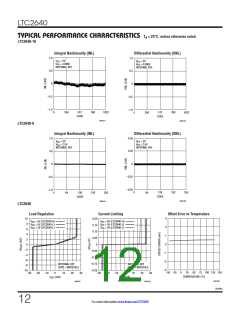
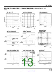
TA = 25°C, unless otherwise noted.
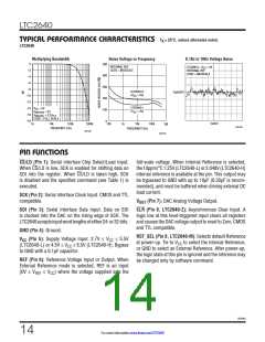
TYPICAL PERFORMANCE CHARACTERISTICS
LTC2640
Multiplying Bandwidth
Noise Voltage vs Frequency
0.1Hz to 10Hz Voltage Noise
0
–2
500
400
300
200
100
0
INTERNAL REF.
CODE = MIDSCALE
LTC2640-L, V = 4V
CC
INTERNAL REF.
CODE = MIDSCALE
–4
–6
–8
LTC2640-H
10µV/DIV
(V = 5V)
–10
–12
–14
–16
–18
CC
LTC2640-L
V
V
V
= 5V
REF(DC)
REF(AC)
CC
(V = 4V)
= 2V
CC
= 0.2V
P-P
CODE = FULL SCALE
1s/DIV
1k
10k
100k
1000k
10k
100
1k
100k
1M
2640 G35
FREQUENCY (Hz)
FREQUENCY (Hz)
2640 G33
2640 G34
PIN FUNCTIONS
CS/LD (Pin 1): Serial Interface Chip Select/Load Input.
When CS/LD is low, SCK is enabled for shifting data on
SDI into the register. When CS/LD is taken high, SCK
is disabled and the specified command (see Table 1) is
executed.
full-scale voltage. When Internal Reference is selected,
the10ppm/°C1.25V(LTC2640-L)or2.048V(LTC2640-H)
internal reference is available at the pin. This output may
be bypassed to GND with up to 10µF (0.33µF is recom-
mended), and must be buffered when driving external DC
load current.
SCK (Pin 2): Serial Interface Clock Input. CMOS and TTL
compatible.
V
OUT
(Pin 7): DAC Analog Voltage Output.
SDI (Pin 3): Serial Interface Data Input. Data on SDI
is clocked into the DAC on the rising edge of SCK. The
LTC2640acceptsinputwordlengthsofeither24-or32-bits.
CLR (Pin 8, LTC2640-Z): Asynchronous Clear Input. A
logic low at this level-triggered input clears all registers
and causes the DAC voltage output to reset to Zero. CMOS
and TTL compatible.
GND (Pin 4): Ground.
REF_SEL (Pin 8, LTC2640-M): Selects default Reference
V
(Pin 5): Supply Voltage Input. 2.7V ≤ V ≤ 5.5V
CC
CC
at power-up. Tie to V to select the Internal Reference,
CC
(LTC2640-L) or 4.5V ≤ V ≤ 5.5V (LTC2640-H). Bypass
CC
or GND to select an External Reference. After power-up,
the logic state at this pin is ignored and the reference may
be changed only by software command.
to GND with a 0.1µF capacitor.
REF (Pin 6): Reference Voltage Input or Output. When
External Reference mode is selected, REF is an input
(0V ≤ V
≤ V ) where the voltage supplied sets the
REF
CC
2640fd
14
For more information www.linear.com/LTC2640

 Linear [ Linear ]