LTC2640
OPERATION
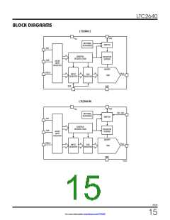
The LTC2640 is a family of single voltage-output DACs
in 8-lead ThinSOT packages. Each DAC can operate rail-
to-rail using an external reference, or with its full-scale
voltage set by an integrated reference. 12 combinations of
accuracy (12-, 10-, and 8-bit), power-on reset value (zero
or mid-scale), and full-scale voltage (2.5V or 4.096V) are
available. The LTC2640 is controlled using a 3-wire SPI/
MICROWIRE compatible interface.
The LTC2640-HM/LTC2640-LM provide an alternative
reset, setting the output to mid-scale when power is first
applied.
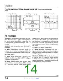
DefaultreferencemodeselectionisdescribedintheRefer-
ence Modes section.
Power Supply Sequencing
The voltage at REF (Pin 6) should be kept within the range
–0.3V ≤ V ≤ V + 0.3V (see Absolute Maximum Rat-
Power-On Reset
REF
CC
ings). Particular care should be taken to observe these
The LTC2640-HZ/LTC2640-LZ clear the output to zero-
scalewhenpowerisfirstapplied,makingsysteminitializa-
tion consistent and repeatable.
limitsduringpowersupplyturn-onandturn-offsequences,
when the voltage at V (Pin 5) is in transition.
CC
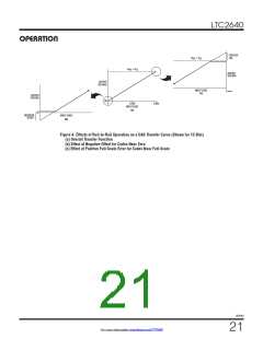
Transfer Function
For some applications, downstream circuits are active
during DAC power-up, and may be sensitive to nonzero
outputs from the DAC during this time. The LTC2640
contains circuitry to reduce the power-on glitch: the
analog output typically rises less than 5mV above zero-
scale during power on if the power supply is ramped
to 5V in 1ms or more. In general, the glitch amplitude
decreases as the power supply ramp time is increased.
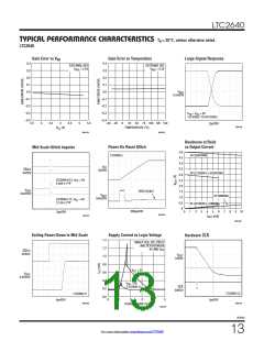
See “Power-On Reset Glitch” in the Typical Performance
Characteristics section.
The digital-to-analog transfer function is:
k
VOUT(IDEAL)
=
V
REF
N
2
where k is the decimal equivalent of the binary DAC input
code,Nistheresolution,andV iseither2.5V(LTC2640-
LM/LTC2640-LZ) or 4.096V (LTC2640-HM/LTC2640-HZ)
when in Internal Reference mode, and the voltage at REF
(Pin 6) when in External Reference mode.
REF
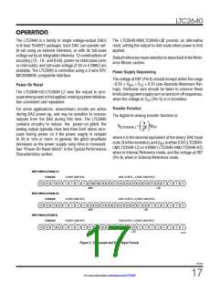
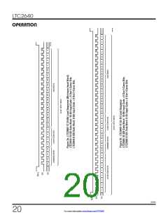
INPUT WORD (LTC2640-12)
COMMAND
4 DON'T-CARE BITS
DATA (12 BITS + 4 DON'T-CARE BITS)
C3 C2 C1 C0
X
X
X
X
D11 D10 D9 D8 D7 D6 D5 D4 D3 D2 D1 D0
X
X
X
X
X
X
X
X
X
X
X
MSB
LSB
INPUT WORD (LTC2640-10)
COMMAND
4 DON'T-CARE BITS
DATA (10 BITS + 6 DON'T-CARE BITS)
C3 C2 C1 C0
X
X
X
X
D9 D8 D7 D6 D5 D4 D3 D2 D1 D0
MSB LSB
X
X
INPUT WORD (LTC2640-8)
COMMAND
4 DON'T-CARE BITS
DATA (8 BITS + 8 DON'T-CARE BITS)
C3 C2 C1 C0
X
X
X
X
D7 D6 D5 D4 D3 D2 D1 D0
MSB LSB
X
X
X
X
X
2640 F02
Figure 2. Command and Data Input Format
2640fd
17
For more information www.linear.com/LTC2640

 Linear [ Linear ]