LT3840
operaTion
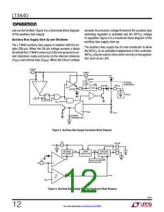
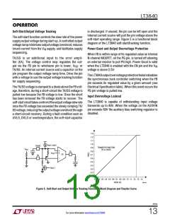
and current limited. Figure 3 is a functional block diagram
of the auxiliary bias supply.
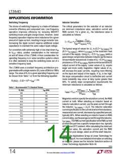
exceeds its precision voltage threshold the auxiliary bias
switching regulator is activated and the INTV voltage
CC
is regulated. Figure 4 is a functional block diagram of the
auxiliary bias supply start-up.
Auxiliary Bias Supply Start-Up and Shutdown
The LT3840 auxiliary bias supply is enabled with the en-
able (EN) pin. When the EN pin voltage exceeds a diode
threshold the LT3840 comes out of the low quiescent cur-
rent shutdown mode and turns on the internal reference
The auxiliary bias supply has its own enable pin to allow
the INTV to be activated independent of the controller.
CC
INTV may be used to drive other circuitry in the applica-
CC
tion such as an LDO.
(V ) and internal bias (V ). When the EN pin voltage
REF
REG
AUXVIN
AUXBST
C
AUXBST
EXTERNAL
COMPONENTS
LPWR
INTV
AUXSW2
CC
AUXSW1
C
INTVCC
R
S
Q
V
> 18V
IN
–
+
V
REF
3840 F03
INTERNAL
COMPENSATION
Figure 3. Auxiliary Bias Supply Functional Block Diagram
V
IN
AUXVIN
INTV
CC
V
V
REG
REF
INTERNAL
REFERENCE
LINEAR
REGULATOR
AUXILIARY
BIAS SUPPLY
–
+
EN
OSCILLATOR
+
–
3840 F04
V
REF
Figure 4. Auxiliary Bias Supply Start-Up Functional Block Diagram
3840fa
12
For more information www.linear.com/LT3840

 Linear [ Linear ]