LT3840
operaTion
low. The V voltage is the DC control node that sets the
age regulator to provide the gate drive voltage from V .
C
IN
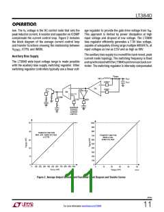
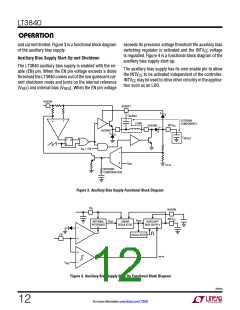
peak inductor current. A resistor and capacitor on ICOMP
compensate the current control loop. Figure 2 includes
the block diagram of the average current control loop
and transfer functions showing the relationship between
This approach is limited by power dissipation at high
input voltage and dropout at low voltage. The LT3840
bias regulator efficiently generates a 7.5V bias voltage,
capable of adequately driving large multiple MOSFETs, at
input voltages as low as 2.5V and as high as 60V.
V
, ICTRL and IMON.
SENSE
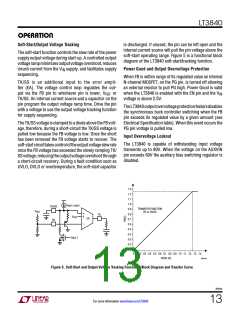
The auxiliary bias supply is a monolithic buck-boost, peak
current mode topology. The switching frequency is fixed
andsynchronizedwiththeLT3840synchronousbuckcon-
troller. The switching regulator is internally compensated
Auxiliary Bias Supply
The LT3840 wide input voltage range is made possible
with the auxiliary bias supply switching regulator. Other
switching regulator controllers typically use a linear volt-
R
SENSE
SW
V
C
OUT
OUT
+
–
SENSE
+
+
20x
SENSE
V
C
+
–
GM
–
1V
–
–
ICOMP
ICTRL
IMON
MAXIMUM
AVERAGE
CURRENT
CONTROL
50
40
1000
900
800
700
600
500
400
300
200
100
0
TRANSFER FUNCTION
MAX. AVG. SENSE VOLTAGE
vs ICTRL
TRANSFER FUNCTION
IMON vs AVG.
SENSE VOLTAGE
30
20
10
0
700 900 1000
800
0
100 200 300 400 500 600
0
10
20
V
30
40
50
V
(mV)
(mV)
ICTRL
3840 F02
SENSE
Figure 2. Average Output Current Limit Functional Block Diagram and Transfer Curves
3840fa
For more information www.linear.com/LT3840
11

 Linear [ Linear ]