LT3840
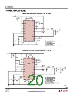
applicaTions inForMaTion
the bulk capacitance and RMS current capability. The bulk
capacitance will determine the supply input ripple voltage.
The RMS current capability is used to prevent overheating
the capacitor. The bulk capacitance is calculated based on
requirements. ΔV
is a function of ΔI and the C
OUT L OUT
ESR. It is calculated by:
1
∆VOUT =∆I • ESR+
L
maximum input ripple, ΔV :
8•f •C
(
)
IN
SW OUT
IOUT(MAX) •VOUT
The maximum ESR required to meet a ΔV
requirement can be calculated by:
design
CIN(BULK)
=
OUT
ΔVIN •fSW •VIN(MIN)
∆V
L f
SW
VOUT
VIN(MAX)
(
)
(
)
(
)
OUT
ΔV is typically chosen at a level acceptable to the user.
IN
ESR(MAX)=
A good starting point is 100mV to 200mV. Aluminum
electrolytic capacitors are a good choice for high voltage,
bulkcapacitanceduetotheirhighcapacitanceperunitarea.
VOUT • 1–
Worst-caseΔV
occursatthehighestinputvoltage.Use
OUT
The capacitor’s RMS current is:
paralleled multiple capacitors to meet the ESR require-
ments. Increasing the inductance is an option to lower the
VOUT(V – V
)
IN
OUT
ICIN(RMS) =IOUT
(V )2
OUT
ESRrequirements.ForextremelylowΔV ,anadditional
IN
LC filter stage can be added to the output of the supply.
Linear Technology’s Application Note 44 has some good
tips on sizing an additional output filter.
If applicable, calculate it at the worst-case condition,
= 2V . The RMS current rating of the capacitor
V
IN
OUT
is specified by the manufacturer and should exceed the
calculated I . Due to their low ESR (equivalent
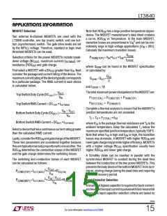
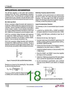
Output Voltage Programming
CIN(RMS)
A resistive divider sets the DC output voltage according
to the following formula:
series resistance), ceramic capacitors are a good choice
for high voltage, high RMS current handling. Note that the
ripplecurrentratingsfromaluminumelectrolyticcapacitor
manufacturersarebasedon2000hoursoflife.Thismakes
it advisable to further derate the capacitor or to choose
a capacitor rated at a higher temperature than required.
VOUT
1.250V
R2=R1
–1
The external resistor divider is connected to the output of
the converter as shown in Figure 6.
The combination of aluminum electrolytic capacitors and
ceramic capacitors is an economical approach to meeting
the input capacitor requirements. The capacitor voltage
L1
V
OUT
rating must be rated greater than maximum V voltage.
IN
R2
R1
C
OUT
Multiple capacitors may also be paralleled to meet size
or height requirements in the design. Locate the capaci-
tor very close to the MOSFET switch and use short, wide
PCB traces to minimize parasitic inductance. Use a small
FB
3840 F06
Figure 6. Output Voltage Feedback Divider
(0.1μF to 1μF) bypass capacitor between the chip V pin
IN
and GND, placed close to the LT3840.
Tolerance of the feedback resistors will add additional er-
Output Capacitor Selection
ror to the output voltage. The V pin input bias current
FB
The output capacitance, C , selection is based on the
is typically 5nA, so use of extremely high value feedback
OUT
design’s output voltage ripple, ΔV
and transient load
resistors results in a converter output that is slightly
OUT
3840fa
16
For more information www.linear.com/LT3840

 Linear [ Linear ]