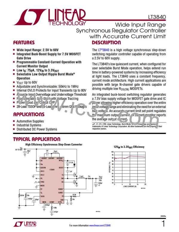
LT3840
pin FuncTions (TSSOP/QFN)
AUXSW1 (Pin 1/Pin 36): AUXSW1 is a switching node of
the auxiliary bias supply. Connect the pin to the auxiliary
bias supply inductor.
OVLO (Pin 11/Pin 12): OVLO has a precision threshold
with hysteresis to implement an accurate overvoltage
lockout (OVLO). Controller switching is disabled during
an overvoltage lockout (OVLO) event. INTV regulation
CC
PGND (Pin 2/Pin 38): PGND is the high current ground
is maintained during an OVLO event. Connect the pin to
GND to disable the function.
return for the auxiliary bias supply. Connect PGND to the
negative terminal of the INTV decoupling capacitor and
CC
to system ground.
UVLO (Pin 12/Pin 13): UVLO has a precision threshold
with hysteresis to implement an accurate undervoltage
lockout (UVLO). UVLO enables the controller switching.
AUXVIN (Pin 3/Pin 1): AUXVIN is the supply pin to the
auxiliary bias supply. Bypass the pin with a low ESR ca-
pacitor placed close to the pin and referenced to PGND.
Connect the pin to V to disable the function.
IN
EN(Pin13/Pin14):ENhasaprecisionICenablethreshold
SYNC (Pin 4/Pin 3): SYNC allows the LT3840 switching
with hysteresis. EN enables the auxiliary bias supply and
frequency to be synchronized to an external clock. Set
controller switching. Connect the pin to V to disable the
IN
the R resistor such that the internal oscillator frequency
T
function. EN also has a lower threshold to put the LT3840
into a low current shutdown mode where all internal cir-
cuitry is disabled.
is 15% below the minimum external clock frequency. If
unused connect the SYNC pin to GND.
RT (Pin 5/Pin 4): An external resistor on RT sets the
switching frequency of the synchronous controller and
auxiliary bias supply.
V (Pin 14/Pin 15): V provides an internal DC bias rail
IN
IN
and should be decoupled to GND with a low value (0.1µF),
low ESR capacitor located close to the pin.
TK/SS(Pin6/Pin6):TK/SSistheLT3840externaltracking
GND (Pin 15, Exposed Pad Pin 29/Pin 17, Exposed Pad
Pin39):Ground. SolderGNDandtheexposedpaddirectly
to the PCB ground plane.
and soft-start input. The LT3840 regulates the V voltage
FB
tothesmalleroftheinternalreferenceorthevoltageonthe
TK/SS pin. An internal pull-up current source is connected
to this pin. A capacitor (C ) to ground sets the ramp rate.
IMON (Pin 16/Pin 18): The voltage on IMON represents
the average output current of the converter. A small value
capacitor filters the ripple voltage associated with the
inductor ripple current.
SS
Alternatively, a resistor divider on another voltage supply
connected to this pin allows the LT3840 output to track
another supply during start-up. Leave the pin open if the
tracking and soft-start functions are unused.
ICTRL (Pin 17/Pin 19): The maximum average output
current is programmed with a voltage applied to ICTRL.
If unused, leave floating.
FB (Pin 7/Pin 7): The regulator output voltage is set with
a resistor divider connected to FB. FB is also the input
for the output overvoltage and power good comparators.
ICOMP(Pin18/Pin20):Acapacitorandresistorconnected
to ICOMP compensates the average current limit circuit.
V (Pin 8/Pin 8): V is the compensation node for the
C
C
output voltage regulation control loop.
+
+
SENSE (Pin 19/Pin 21): SENSE is the positive input for
PG (Pin 9/Pin 9): PG is a power good pin and is the open-
drain output of an internal comparator.
the differential current sense comparator.
–
–
SENSE (Pin 20/Pin 22): SENSE is the negative input for
MODE (Pin 10/Pin 11): MODE is used to enable or disable
Burst Mode operation. Connect MODE to ground for Burst
Mode operation. Connect the pin to FB for pulse-skipping
the differential current sense comparator.
SW (Pin 21/Pin 24): SW is the high current return path
of the TG MOSFET driver and is externally connected to
the negative terminal of the BOOST capacitor.
mode. Connect MODE to INTV for continuous mode.
CC
3840fa
For more information www.linear.com/LT3840
7

 Linear [ Linear ]